1 Introduction
Data acquisition is an effective method for analyzing analog signal volume data. The real-time display of data is the actual demand of automated inspection systems. In the process of testing the seeker of the air-to-air missile, the response signal of the seeker includes the internal secondary power signal and the analog voltage signal. During the detection process, the detection system is required to display the working status of the seeker in real time, display the secondary power supply and analog response voltage signal, judge the performance of the seeker, and ensure that the seeker is artificially dealt with emergency treatment under extraordinary circumstances to protect the guidance. Lead. For the analog voltage signal, it is usually realized by the method of analog-to-digital conversion and post-data calibration. According to the actual needs, the corresponding detection system can be developed as an important tool for the daily maintenance and repair of the seeker. Here is a design scheme of real-time data acquisition and display system based on single-chip microcomputer and CPLD.
2 System composition
There are 16 channels of voltage signals to be collected and displayed in this system, and the dynamic voltage range is -22~+27 V. Since these voltage signals have a low frequency of change, or it is considered that the frequency does not change, and the detection system only cares about its voltage value, the system requirements can be met at a low sampling rate. According to the demand, the sampling rate designed by the system, that is, the display refresh rate is above 1.56 k/s.
The single-chip 80C196KB and programmable logic device EPM7128SLC are used as the core controller, and the 80C196KB internal integrated A/D converter is used as the analog-to-digital converter to realize the real-time data acquisition, display and control of 16 voltage signals. The block diagram of the overall design of the system is shown in Figure 1.
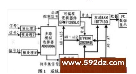
The whole system is mainly composed of signal preprocessing, signal gating, single-chip acquisition, dual-computer data transmission and data processing and display modules. Among them, the signal strobe module is composed of CPLD and multiple analog selectors.
3 System hardware circuit design
3.1 Signal preprocessing circuit
Because the voltage signal to be collected has a wide input dynamic range and different polarity, for the single-chip A/D converter, it needs to be adjusted to the voltage range of 0~5 V that can be collected, so it is necessary to uniformly adjust the collected signal, as shown in the figure 2 shown.
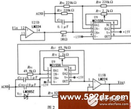
The op amps LM224 and MC1556 in Figure 2 both use dual-voltage power supply to increase the dynamic signal input range; the resistors use precision metal film resistors with an accuracy of 0.1% to improve voltage conversion accuracy.
In the process of secondary voltage regulation, the MC1556 non-phase input terminal adopts a voltage stabilizing circuit to reduce the adverse effect of temperature rise on the system when the power is turned on for a long time. Nanyu voltage follower has the characteristics of large input impedance and strong output driving ability, so voltage follower circuits are used at the input and output ends of the preprocessing circuit.
3.2 Signal strobe circuit
ADG508A is an 8-channel CMOS analog multiplexer with high-speed conversion speed and low internal resistance. The channel switching has the function of preventing short-circuit. Under CPLD control, it can perform orderly channel switching on the acquisition signal, and cooperate with the single-chip microcomputer for data acquisition.
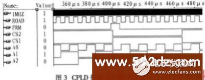
EPM7128SLC is a CPLD produced by Ahera, with a capacity of 128 macrocells. It uses the hardware description language VHDL to program the CPLD to achieve signal strobe control. Firstly, compile the frequency divider module to divide the frequency of the 1 MHz crystal oscillator by 20, and output 2 rectangular synchronization signals with phase shift and a period of 20 μs. One of the signals is divided by 2 by the D flip-flop to obtain a square wave signal with a duty ratio of 50% and a period of 40 μs; then the signal gating control module is programmed. This module cyclically outputs control signals based on the square wave signal and another synchronization signal. Both modules are developed in the MuxPlus-II environment. The timing simulation results of the CPLD control signal are shown in Figure 3. Among them, the signals FRM and ROAD are the main program of the single-chip microcomputer. The service signal; CS1 and CS2 are the chip selection signals of the two ADG508A: A0, A1 and A2 are the ADG508A channel strobe control signals.
3.3 Single-chip acquisition circuit
80C196KB is a 16-bit CMOS single-chip microcomputer produced by Intel, with 8 A/D converters integrated on-chip. The converter includes an 8-channel multiplexed analog switch, sample-and-hold circuit and 10-bit A/D converter. Because there is a multiplexer outside the system, there is no need for channel conversion inside, and data acquisition can be completed by using an ACH0 channel. As to the one-chip computer system adopting 12 MHz crystal oscillator, it takes 22μs to complete an A/D conversion. The 80C196KB A/D converter uses the method of successive approximation to complete the conversion from analog to digital. The reference voltage setting is very critical. The internal resistance-capacitance network divides the reference voltage Vref into 1,024 steps, each of which is Vref/1 024 V. By comparing with the reference voltage, a 10-bit data conversion result can be obtained. The accuracy and stability of the reference voltage directly affect the absolute accuracy of the measurement result. Therefore, in the circuit, Vref is powered by a separate power supply and the accuracy and stability are improved by the reference voltage source such as 5 V of LM136.
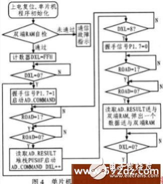
80C196KB reads the last A/D conversion result by judging the ROAD signal on its rising edge, and starts the A/D converter to convert the next signal. The single-chip microcomputer uses the FRM signal as a non-masked interrupt to reset the counter DXL to zero, and the main program loops once , To ensure the time-division multiplexing acquisition of 16-channel signals. The program flow of the one-chip computer 80C196KB is shown as in Fig. 4.
3.4 Double machine data transmission
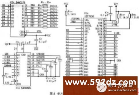
In order to achieve the real-time controllability of the collected data, the system designs a dual-computer communication interface as a channel for transmitting the A/D conversion data of the single-chip microcomputer to the computer. The computer adopts EPP mode communication under WDM, and the speed can reach 500 KB/s~2 MB/s. Using dual-port RAM IDT7130 as the main component, through the communication interface, the one-chip computer stores the A/D conversion data in the dual-port RAM, and the computer displays the data read from the dual-port RAM in real time. The one-chip computer carries on the write operation through the A port of the dual-port RAM IDT7130, and the computer carries on the read operation through the B port. The handshake signal is generated by the single-chip microcomputer by counting the ROAD signal, and the two can read and write asynchronously to realize data exchange. Figure 5 shows the interface circuit between the microcontroller and the computer.
4 System software design
4.1 Data calibration
Given Vref=5 V, suppose the input voltage of the one-chip computer acquisition port is Vin and the corresponding A/D conversion digital quantity is X, then X=1 024 Vin/5V. For the linear conversion pre-processing circuit, Y=5KX/1 024 can be used, where Y represents the measured voltage value, X represents the A/D conversion value corresponding to Y, and K is the amplifier gain. Let K=Ymax/5 V, where Ymax represents the maximum value of the voltage to be measured. In order to ensure the accuracy of acquisition, Ymax should be calculated first to maintain sufficient A/D conversion effective figures. Take the voltage 0~27 V to be collected as an example, the gain of the preprocessing circuit is 27/5=5.4.
4.2 Real-time display
The reading and display software is written in VC++6.0 environment, using dialog mode, and the parallel port adopts WDM drive mode. When the software is running, directly open the drive device, and at the same time use the AfxBeginThread() function to generate a new thread, and its control thread function updates in real time to read and display the data. Because the one-chip computer adopts 1O-bit A/D converter, the result of one conversion is transmitted twice, which are high-order and low-order transmissions. Parallel port data transmission also adopts 8-bit mode. After the host computer reads the data, two sets of data are shifted and added to obtain a complete data, which is displayed on the computer interface after calibration.
5 Conclusion
Practice has proved that the real-time acquisition and display system fully meets the detection requirements of the seeker. The accuracy of the collected voltage is up to mV, and the refresh rate is above 1.56 k/s. The system uses single-chip microcomputer and CPLD technology, the circuit design structure is simple, the actual application reliability is high, the versatility is strong, the use is flexible, and the acquisition channel is expandable. But in the circuit design process, attention should be paid to: because the system has both analog and digital circuits, reasonable wiring is very important to the system. Reasonable wiring measures should be taken to ensure the stability of the reference ground, thereby improving the accuracy of acquisition.
Genuine Flip Cover Leather Case
Genuine Flip Cover Leather Case,Cover Leather Case,Flip Cover Leather Case,Genuine Leather Case
Guangzhou Jiaqi International Trade Co., Ltd , https://www.make-case.com