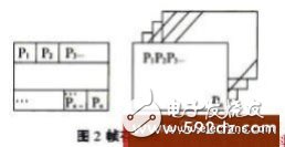
There are two ways to organize the memory (Figure 2): â‘ Packed Pixel Method: that is, all the bits of each pixel on the screen are stored in a single memory bank; â‘¡Bit Plane Method: namely Each bit of the pixel is stored in a different memory bank. Due to the use of multiple memory banks, they can read out more pixel information at the same time. From the analysis of the two storage structures, the use of the bit plane structure is beneficial to improve the display effect of the LED screen.

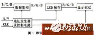
The structure block diagram of the entire LED display screen display control circuit is shown in Figure 3. Among them, the data reconstruction circuit completes the conversion of RGB data, combines the same weight bits of different pixels together, and then stores them in adjacent cells, thereby completing the recombination of the entire data in the form of bits.

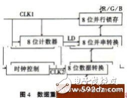
The data reconstruction circuit is mainly composed of four parts: 8-bit data parallel transmission circuit; 8-bit parallel-serial conversion circuit; 8-bit data latch circuit; 8-bit plus 1 counter. Each 8-bit data of R/G/B is input into the parallel latch by the pixel frequency after synchronization processing, the 8-bit plus 1 counter outputs the carry pulse LD, and the 8-bit data is simultaneously latched to the 8-bit parallel-serial conversion circuit , The clock control circuit completes the parallel-serial conversion circuit clock control. After the data is reconstructed, there is no longer a pixel value in a memory bank, but the same weight bits of different pixel values. Store all the same-weight bits together to form a bit-plane storage structure in units of bits. When reading out, the adjacent weight of each pixel must be taken out according to the opposite rule.

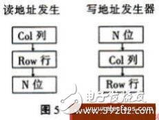
The read and write address generator must meet strict timing. For the same memory chip, it can be divided into N slices (a pixel value is represented by N bits), and each slice represents a bit plane. When the pixel is converted to the same memory, write 0 bit and then write 1 bit. , And finally write N bits. For an 8Col×Row dot matrix display screen, each bit plane stores 8Col×Row bits. The internal organization of the memory depends on the logical connection of the pixel tubes on the drive screen. According to the memory organization, the read address generator is driven by columns, and then bits are driven by rows; the write address generator is driven by bits to drive columns and columns to drive rows, which can ensure read and write synchronization and display the original image correctly and synchronously. letter.

SHAOXING COLORBEE PLASTIC CO.,LTD , https://www.fantaicolorbee.com