1 Overview
2 POE main power supply characteristics
2.1 PSE characteristic parameters
2.2 PD power level
2.3 Working process of POE power supply
3 Introduction to POE Power Module
3.1 POE power module chip
3.2 Introduction to input circuit and output circuit
3.3 Introduction to chip peripheral circuits
3.4 Selection of transformer and switch tube
4Power PDN and ripple noise
4.1 Power PDN
4.2 Power supply ripple and power supply noise
5Common Ripple and Noise Test Schemes
5.1 Basic requirements for ripple and noise testing
5.2 High-pass filter characteristic analysis
5.3 Passive probe DC coupling test
5.4 Passive probe AC ​​coupling test
5.5 Coaxial line external DC blocking capacitor DC50 ohm coupling test
5.6 Coaxial line AC1M ohm coupling test
5.7 Differential probe external capacitance DC coupling test
5.8 Differential probe attenuation DC coupling test
6 Power module voltage test
6.1 Input voltage measurement
6.2 Output voltage measurement
7 summary
1 Overview:
Definition: The full name of PoE is Power Over Ethernet, which refers to 10BASE-T, 100BASE-TX, 1000BASE-T Ethernet network power supply, that is, the data cable and power cable are transmitted on the same network cable, and the longest reliable power supply distance is 100 meters.
The PoE power supply system includes two types of equipment, PSE and PD, PSE (power-sourcing equipment), which is mainly used to supply power to other equipment, and PD (power device), which is used to receive power in the PoE power supply system.
2 POE main power supply characteristics
2.1 PSE characteristic parameters:
(1) The voltage is between 44~57V, the typical value is 48V
(2) The maximum allowable current is 550mA, and the maximum starting current is 500mA
(3) Typical working current is 10~350mA, overload detection current is 350~500mA
(4) Under no-load conditions, the maximum required current is 5mA
2.2 PD power level
PD power level is divided into CLASS 0, CLASS 1, CLASS 2, CLASS 3, CLASS 4, CLASS 5
The maximum working power required by CLASS 0 equipment is 0.44W ~ 12.95W
The highest working power required by CLASS 1 equipment is 0.44W ~ 3.84W
The highest working power required by CLASS 2 equipment is 3.84W ~6.49W
The highest working power required by CLASS 3 equipment is 6.49W ~ 12.95W
The highest working power required by CLASS 4 equipment is 12.95W ~ 25.5W
The maximum working power required by CLASS 5 equipment is >25W
Designers can assign their equipment to specific levels based on power requirements.
2.3 Working process of POE power supply
In the classification stage, PSE will apply a voltage of 15-20V to the PD and determine the specific level of the PD by measuring the current. At this stage, the power part of the PD will be maintained in a passive state by an undervoltage lockout (UVLO) circuit to isolate the switch stage until the characterization and classification stages are completed. Once the classification is completed, the PSE will provide the full working voltage to the PD. When arranging PSE power supply terminal equipment in a network, the working process of POE Power over Ethernet is as follows:
Detection:
First, the PSE will send a test voltage to the network device to detect a 24.9kΩ common-mode resistance in the powered device. The test signal starts at 2.5V and then increases to 10V, which will help compensate for the loss caused by the impedance of the Cat-5 cable itself. Because this cable can be up to 100m long. If the PSE detects the appropriate impedance characteristic (24.9kΩ) from the PD, it will continue to increase the voltage. If the characteristic impedance cannot be detected, the PSE will not power up the cable. The Zener diode in the circuit of the powered device will ensure that the rest of the system is not interfered by the test signal.
PD device classification:
After detecting the power receiving device PD, the PSE will apply a voltage of 15-20V to the PD and determine the specific level of the PD by measuring the current. If no other classification circuit is found except the resistance of the first level, the device is defined as zero level. At this stage, the power part of the PD will be maintained in a passive state by an undervoltage lockout (UVLO) circuit to isolate the switch stage until the characterization and classification stages are completed.
Start power supply:
After the classification is completed, within a start-up period of a configurable time (generally less than 15μs), the PSE device starts to supply power to the PD device a) from a low voltage until it provides a 48V DC power supply. b) Power supply: Provide a stable and reliable 48V DC power for PD equipment to meet the power consumption of PD equipment that does not exceed 12.95W. c) Power failure: When the PD device is disconnected from the network, the PSE will quickly (usually within 300-400ms) stop powering the PD device, and repeat the detection process to detect whether the cable terminal is connected to the PD device.
3 Introduction to POE Power Module
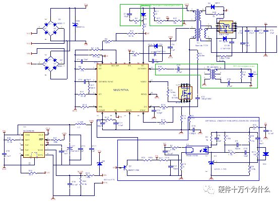
This time, the POE power supply module adopts MAX5969B and MAX5974A chips to realize the POE power supply with a power level of CLASS 4. The circuit topology of the POE power module is realized by a flyback converter, using transformer primary side feedback voltage stabilization and secondary side synchronous rectification technology. The input voltage range is between 36V and 57V, the output voltage is stable at 5V, and it has the characteristics of overvoltage protection and overcurrent protection. Figure 1 shows the schematic diagram of the POE power supply.
3.1 POE power module chip
The chip MAX5969B provides a complete interface that complies with the IEEE802.3af/at standard of the Power-over-Ethernet (PoE) system for PDs. MAX5969B provides detection signal, classification signal and integrated isolation power switch with inrush current control for PD. During a surge, the MAX5969B limits the current to less than 180mA until the isolation power MOSFET is fully turned on and then switches to a higher current limit (720mA to 880mA). The device has an input UVLO with a wide hysteresis and long-period interference pulse shielding to compensate for the resistive attenuation of twisted-pair cables and ensure interference-free transmission during power-up/power-down. The MAX5969B input can withstand voltages up to 100V.
The MAX5969B chip features are as follows:
(1) Compatible with IEEE 802.3af/at
(2) Level 2 incident classification
(3) Simple wall adapter interface
(4) 0 to 5 POE classification
(5) 100V absolute maximum rated input
(6) 180mA maximum surge current limit
(7) The current is limited to 720mA to 880mA during normal operation
(8) Current limit and foldback protection
(9) Traditional 36V UVLO (MAX5969A)
(10) IEEE 802.3af/at compatible, 40V UVLO (MAX5969B)
(11) Overheat protection
(12) 3mm × 3mm, 10-pin TDFN package with enhanced heat dissipation
Figure 2 shows the pin diagram of MAX5969B, and then briefly introduce each pin.
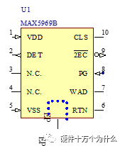
Figure 2 MAX5969B pin diagram
Table 1 MAX5969B pin introduction
| Pin | name | Features |
| 1 | VDD | Positive power input. Connect a 68nF (minimum) bypass capacitor between VDD and VSS. |
| 2 | DET | Sense resistance input. Connect a characteristic resistor (RDET = 24.9kΩ) between DET and VDD. |
| 3 | NC | No connection, no internal connection. |
| 4 | IC | Internally connected, floating. |
| 5 | VSS | Negative power input. VSS is connected to the source of the integrated isolation n-channel power MOSFET. |
| 6 | RTN | Isolate the drain of the MOSFET. RTN is connected to the drain of the integrated isolation n-channel power MOSFET, and RTN is connected to the ground of the subsequent DC-DC converter. |
| 7 | WAD | Wall power adapter detector input. When VDD-VSS exceeds the mark event threshold, the wall adapter detection is enabled. When the voltage between WAD and RTN is greater than 9V, it will be detected. When connecting the wall power adapter, disconnect the isolated n-channel power MOSFET and turn on the 2EC current sink circuit. When not using a wall power adapter or other auxiliary power source, connect the WAD directly to the RTN. |
| 8 | PG | Power ready indication open drain output. When the hot-swap MOSFET switch is turned on, PG will absorb 230μA current to disable the subsequent DC-DC converter until the hot-swap switch is fully turned on. In detection, classification and regulated power supply modes, PG current sinking is prohibited. |
| 9 | 2EC | Active low level 2 event level detection or wall adapter detection output. When a Type 2 PSE or wall adapter is detected, the 1.5mA sink current at 2EC is enabled. When powered by a Class 2 PSE, after the isolation MOSFET is fully turned on, the 2EC current sink is enabled and locked to a low level until VIN drops below the UVLO threshold. When the wall adapter power (usually greater than 9V) is applied between WAD and RTN, 2EC will also be effective. When WAD triggers 2EC, 2EC will not be locked. |
| 10 | CLS | Grading resistance input. Connect a resistor (RCLS) between CLS and VSS to set the required classification current. Regarding the resistance value corresponding to a specific PD classification,. |
| –– | EP | Exposed pad. Do not use EP as the electrical connection of VSS, EP passes |
A brief introduction to the working process of the chip MAX5969B, MAX5969B has 4 different working modes:
PD detection, PD classification, marking event and PD power supply mode. The detection mode is used to detect whether the device is a PD device; the classification mode is used to determine the input power for the PD device; the mark event is generally used for the detection of the 2-level classification mode; the power supply mode is to formally power the PD device.
When the input voltage is between 1.4V and 10.1V, the device enters the PD detection mode; when the input voltage is between 12.6V and 20V, the device enters the PD classification mode; once the input voltage exceeds VON, the device enters the PD power supply mode.
Detection mode (1.4V≤ VIN ≤ 10.1V):
In the detection mode, the PSE applies two voltages ranging from 1.4V to 10.1V (with a minimum step of 1V) to VIN, and records the current measurement values ​​at these two points. Then, the PSE calculates DV/DI to ensure that the 24.9kΩ characteristic resistor is connected. Connect a characteristic resistor (RDET) between VDD and DET to ensure correct characteristic detection. In detection mode, MAX5969B pulls DET low. When the input voltage exceeds 12.5V, DET becomes high impedance. In the detection mode, most of the internal circuits of MAX5969B are in the off state, and the bias current is less than 10μA.
Classification mode (12.6V≤ VIN ≤ 20V):
In the classification mode, the PSE classifies the PD according to the power consumption required by the PD, so that the PSE can effectively manage the power allocation. The definition of levels 0 to 5 can be known by viewing the data sheet (the IEEE 802.3af/at standard only defines levels 0 to 4, and level 5 is for special requirements). An external resistor (RCLS) is connected between CLS and VSS to set the classification current. The PSE determines the level of the PD by applying a voltage to the input of the PD and measuring the current output by the PSE. When the voltage applied by the PSE is between 12.6V and 20V. PSE uses classification current information to classify PD power requirements. The classification current includes the current absorbed by the RCLS and the supply current of the MAX5969B. Therefore, the total current absorbed by the PD is within the range of the IEEE 802.3af/at standard. When the device is in power supply mode, the classification current is turned off.
Power supply mode (wake-up mode)
When VIN rises above the undervoltage lockout threshold (VON), the MAX5969B enters power supply mode. When VIN rises above VON, the MAX5969B turns on the internal n-channel isolation MOSFET, connects VSS to RTN, and sets the internal inrush current limit to 135mA (typical). When the voltage at RTN approaches VSS and the surge current drops below the surge threshold, the isolation MOSFET is fully turned on. Once the isolation MOSFET is fully turned on, the MAX5969B changes the current limit to 800mA. Before the power MOSFET is fully turned on, the power-ready open-drain output (PG) remains low for at least a duration to disable the subsequent DC-DC converter during the surge. The chip also has some other working states, such as under-voltage lockout, thermal shutdown protection, wall power adapter detection and work, etc.
The chip MAX5974A is a wide input voltage range, active clamp, current-mode PWM controller, used to control the forward converter in Power-over-Ethernet (PoE) powered devices (PD). The MAX5974A is suitable for the input voltage range of general-purpose or telecommunication systems. The unique circuit design of the chip MAX5974A can obtain stable output without the need for optocouplers.
MAX5974A has many features, here are a few briefly introduced:
(1) Peak current mode control, active clamp, forward PWM controller
(2) Regulated output can be obtained without optocoupler
(3) 100kHz to 600kHz programmable, ±8% jitter control switching frequency, can be synchronized up to 1.2MHz
(4) Programmable frequency jitter, support low EMI, spread spectrum work
(5) Programmable dead time, PWM soft start, current slope compensation
Figure 3 shows the pin diagram of the chip.
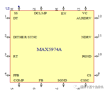
Figure 3 MAX5974 pin diagram
Table 2 MAX5974A pin introduction
| Pin | name | Features |
| 1 | DT | Resistor connection for dead time programming. Connect resistor RDT from DT to GND to set the dead time between the NDRV and AUXDRV signals. Refer to the dead time section to calculate the resistance value corresponding to the specific dead time. |
| 2 | DITHER/ SYNC | Frequency plus jitter programming or synchronous connection. For spread spectrum operation, connect a capacitor from DITHER to GND and a resistor from DITHER to RT. To synchronize the internal oscillator to an externally provided frequency, connect DITHER/SYNC to the sync pulse. |
| 3 | RT | Switching frequency programming resistor connection. Connect resistor RRT from RT to GND to set the PWM switching frequency. Refer to the oscillator/switching frequency section to calculate the resistance value corresponding to the specific oscillator frequency. |
| 4 | FFB | Frequency foldback threshold programming input. Connect a resistor from FFB to GND to set the output average current threshold. Below this threshold, the converter folds back the switching frequency to 1/2 of its original value. When this pin is connected to GND, the frequency foldback function is disabled. |
| 5 | COMP | Transconductance amplifier output and PWM comparator input. Use a level shifter to convert COMP to a low level and connect it to the inverting input of the PWM comparator. |
| Pin | name | Features |
| 6 | FB | Transconductance amplifier inverting input. |
| 7 | SGND | Signal ground. |
| 8 | CSSC | Current detection with slope compensation input. The resistor connected between CSSC and CS is used to set the slope compensation amount. |
| 9 | CS | Current detection input. Current detection connection for average current detection and cycle-by-cycle current limit. The peak current limit trigger voltage is 400mV, and the reverse current limit trigger voltage is -100mV. |
| 10 | PGND | Power ground. PGND is the switching current loop of the gate driver. |
| 11 | NDRV | Main switch gate driver output. |
| 12 | AUXDRV | PMOS active clamp switch gate driver output. AUXDRV can also drive pulse transformers for synchronous flyback applications. |
| 13 | IN | Converter power input. IN has wide UVLO hysteresis, enabling high-efficiency power supply design. When using the enable input EN to set the UVLO level of the power supply, connect a Zener diode between IN and PGND to ensure that VIN is always clamped below its absolute maximum rating of 26V. |
| 14 | EN | Enable input. When the EN voltage is lower than VENF, the gate driver is disabled and the device is in low-power UVLO mode. When the EN voltage is higher than VENR, the device checks other enable conditions. |
| 15 | DCLMP | Feedforward maximum duty cycle clamp programming input. Connect a resistor divider between the input supply voltage DCLMP and GND. The voltage on the DCLMP sets the maximum duty cycle (DMAX) of the converter, which is inversely proportional to the input supply voltage, so the MOSFET is still in a protected state during transients. |
| 16 | SS | Soft start programming capacitor connection. Connect a capacitor between SS and GND to set the soft-start period. This capacitor also determines the restart time of the hiccup mode current limit. The resistor between SS and GND can also be used to set DMAX below 75%. |
| — | EP | Exposed pad. Internally connected to GND. Connect to a large ground area to enhance heat dissipation. Do not use it as an electrical connection point. |
3.2 Introduction to input circuit and output circuit
The input voltage is taken from the 48V power supply of the network port, and the input voltage passes through two rectifier bridges D1 and D2, where D26 is a transient suppression diode SMBJ54A to protect the input from overvoltage.
The output voltage is obtained after rectification on the secondary side of the flyback transformer. Because the pulsating voltage after rectification is large, an output filter capacitor will be added after rectification. The output filter capacitor will generally choose several large capacitors and a small capacitor in parallel. Play the role of energy storage and filtering, small capacitors are used for high frequency decoupling, and several capacitors in parallel can minimize the output resistance. The POE power supply of this module chooses 3 ceramic capacitors with a package of 1206 and a capacitance of 47uF. The flyback transformer chooses the SIR412DP switch tube to realize active rectification, and uses the transformer secondary winding to obtain the driving voltage, so that the primary side of the transformer does not need a degaussing circuit or absorption circuit, but uses energy to drive the SIR412DP switch tube to achieve synchronous rectification technology . The drain and source of the switch tube are connected in parallel with an RCD absorbing circuit to suppress the voltage spike at the drain-source terminal of the switch tube to achieve the purpose of protecting the switch tube. Although the MOSFET is a voltage-controlled switching tube, the switching tube is turned on and off by charging the parasitic capacitance of the switching tube to turn it on or off, which requires a certain drive current. So connect a 10 ohm resistor in series with the drive circuit.
3.3 Introduction to chip peripheral circuits
The main function of the chip MAX5969B is the chip used to communicate with the PSE power supply module when it is just powered on. For every POE power supply, this similar chip is essential. Some of the so-called POE power supplies on the market often just change the 48V voltage to 5V or other voltages. There is no detection and classification stage when the power is turned on, which is dangerous for the power receiving equipment. The general method to detect whether the power supply is a POE power supply or a non-POE power supply is to measure the power supply pins with a multimeter, usually pins 4, 5, 7, and 8 of the network port. If the port output is a stable 48V voltage, this indicates that the power supply is a non-POE power supply; If the measured voltage jumps between 2~10V, it means that the power supply is a POE power supply, and the voltage jump is detected on the PD end.
The VDD of the chip MAX5969B is the power supply pin. A 0.1uF capacitor is connected between VDD and VSS for bypass, and capacitors C7 and C13 are used for energy storage and filtering.
DET connects a 24.9K resistor to Vin. The characteristic resistance of this resistor cannot be changed. If the resistance value of this resistor is changed, the POE power supply will not work normally.
The VSS pin is connected to the ground terminal after input rectification, and the VSS is internally connected to the ground terminal of the primary side of the transformer through the MOSFET tube. When the chip is in the detection and classification stage, the internal MOSFET is in an off state.
The RTN pin is connected to the ground terminal of the primary side of the transformer, which is the power ground terminal of the subsequent DC-DC.
The WAD pin is used to connect to the wall adapter power supply. The POE power supply of this module does not use the wall adapter, but it is also considered in the circuit design, but there is no welding related components.
The internal PG pin is the MOSFET drain output. Before the MOSFET inside the chip is completely turned on, PG remains low, and the PG terminal is connected to the enable terminal of MAX5974A. Therefore, MAX5974A is in a non-working state during the period when PG remains low. . PG is bypassed with an external 1nF capacitor.
The 2EC pin is a level 2 event detection pin. This module does not directly pull up a 100K resistor to RTN to prevent the 2EC pin from having a loop when the PD device is in the level 2 state.
The CLS pin is a grading resistance input pin. How much resistance is connected to the CLS pin to the VSS ground terminal determines which level the POE power supply is at. You can check the data sheet to know that when a 30.9 ohm resistor is connected, the PD device is set to a level 4 circuit state, which means that the PD device consumes 12.95-25.5W of power.
The chip MAX5974A is a power management chip with many functions integrated inside the chip. As long as you follow the peripheral circuit construction method recommended in the chip data manual, you can quickly design a power module by simply configuring some capacitors and resistors. Next, we will introduce the construction of the peripheral circuit of each pin of the chip to better understand the chip and the flyback switching power supply.
The DT pin is used to set the dead time. Because the MAX5974A chip provides two gate driver outputs, one is the NDRV main switch gate driver output, which is used to drive whether the primary side of the transformer is off or out Connected state. One is that AUXDRV is a drive signal used to achieve synchronous rectification for the secondary side switch tube of the transformer. Because the primary side switch tube of the transformer and the secondary side switch tube of the transformer cannot be turned on at the same time, although NDRV and AUXDRV are complementary output, but because of the switch tube itself The turn-on and turn-off process is not ideal, there is a certain time delay when turning on and off, so a certain dead time needs to be added. The dead time setting time is between 40ns and 400ns. The dead time is set by connecting a resistor to the RTN ground terminal. The specific resistance setting and the long dead time can be obtained by the following formula:
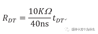
The module selection=27KW, the dead time is 108ns, which is enough for this dead time, because the delay time of the MOSFET used this time is within 40ns.
The DITHER/SYNC pin is the frequency plus jitter programming or synchronization connection pin. Connect a capacitor between DITHER/SYNC and RTN ground, and connect a resistor between DITHER/SYNC and RT, which can jitter the switching frequency of the converter within the range, thereby reducing EMI. The specific process is that the current source at DITHER/SYNC charges the capacitor C14 to 2V with a current of 50uA. After reaching this point, discharge C14 to 0.4V with a current of 50uA. Capacitor charging and discharging will generate a triangular wave on DITHER/SYNC with peak values ​​of 0.4V and 2V respectively. Normally, the frequency is 1KHZ. The calculation formula of capacitor C14 is:
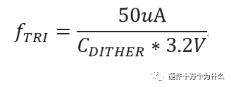
This module chooses C14=10nF, and the connection resistance formula is as follows:

Among them, %DITHER is the amount of dithering, expressed as a percentage of the switching frequency. Setting RDITHER to 10 RRT produces a jitter of ±10%. There is no secondary resistance for welding in this module, but a place is reserved, and the last resistance can be welded when needed.
The RT pin is the switching frequency programming resistor connection. Connect to RTN ground and set PWM switching frequency between 100KHZ~600KHZ. You can refer to the following formula:
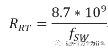
For the switching frequency of the PWM wave, the power supply of this module is 29.4K, which means that the switching frequency is 296KHZ.
The FFB pin is the frequency foldback threshold programming input. Connect a resistor from FFB to RTN ground to set the output average current threshold. Below this threshold, the converter folds back the switching frequency to 1/2 of its original value. When this pin is connected to RTN ground, the frequency foldback function is disabled. The function of this pin is to reduce the switching frequency when the load is light, so as to reduce the switching loss, improve the converter efficiency, and save energy. The connected resistance calculation can be obtained by the following formula:

Among them, RFFB is the resistance between FFB and RTN ground, ILOAD (LIGHT) is the current that triggers frequency foldback under light load conditions, RCS is the detection resistance connected between CS and RTN ground, and IFFB is the source of FFB to RFFB. Current (30µA, typical). This module is connected through a 0 ohm resistor.
The COMP pin is the output of the transconductance amplifier and the input of the PWM comparator. Use a level shifter to convert COMP to a low level and connect it to the inverting input of the PWM comparator. This pin is used to improve the loop stability and make the output voltage stable and ripple small. This module adopts the second type loop compensation network to realize the stability of the loop, which is specifically completed by the circuit composed of C15, C16 and R10 in the schematic diagram.
The FB pin is the inverting input of the transconductance amplifier. The MAX5974A contains an internal error amplifier with sample-and-hold input. The non-inverting input of the error amplifier is connected to the internal reference and feedback is provided at the inverting input. High open-loop gain and unity gain bandwidth can achieve good closed-loop bandwidth and transient response. Use the following formula to calculate the output voltage coupled to the primary side of the transformer:
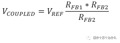
The MAX5974A is 1.52V, and the feedback voltage can be obtained by the following formula:

Of this module

The feedback voltage of this module is taken from the voltage coupled to the primary side of the transformer, instead of using the traditional scheme of using TL431 and PC817 to obtain the feedback voltage so as to stabilize the output voltage, but the TL431 and PC817 feedback are also reserved during the circuit design. The program to obtain stable output voltage. Another function of the voltage coupled to the primary side of the transformer is to provide power input to the MAX5974A chip. The output voltage can be changed by setting the voltage of the feedback part, which can be known from the following formula:

Among them, VOUT is the output voltage, NC/NO is the turns ratio of the coupled output and the main output winding. The turns ratio is selected so that VCOUPLED is higher than the UVLO turn-off level (7.35V, maximum) by a certain margin, which is determined by the hold time required to "cross" a power-down. The SGND pin is the signal ground pin connected to the RTN ground.
CSSC pin has current detection with slope compensation input. The resistor connected between CSSC and CS is used to set the slope compensation amount. The device generates a current ramp on the CSSC terminal, the peak value of which reaches 50μA when the oscillator duty cycle is 80%. An external resistor connected from CSSC to CS converts the current ramp to a programmable slope compensation amplitude, which is added to the current detection signal to stabilize the peak current mode control loop. The rate of change of the slope compensation signal is given by:
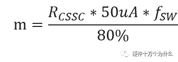
Among them, m is the rate of change of the slope compensation signal; RCSSC is the resistance value connected between CSSC and CS to set the rate of change; fSW is the switching frequency. The resistance R18 of this module is 4.02K.
The CS pin is the current sense input. Current detection connection for average current detection and cycle-by-cycle current limit. The peak current limit trigger voltage is 400mV, and the reverse current limit trigger voltage is -100mV. The current sense resistor (RCS in the typical application circuit) connected between the source of the n-channel MOSFET and the RTN ground is used to set the current limit. The voltage trigger level (VCS-PEAK) of the current-limiting comparator is 400mV. Use the following formula to calculate the RCS value:
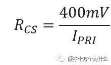
Among them, IPRI is the peak current of the primary side of the transformer, which also flows through the MOSFET. When the voltage generated by this current (through the current sense resistor) exceeds the current limit comparator threshold, the MOSFET driver (NDRV) terminates the current conduction cycle within 35ns (). The current-limiting resistor of this module chooses R21 and R25 as 1206. The package resistance value is 0.25 ohm. Using a small RC network, additional filtering is performed on the leading edge spikes on the detected waveform. The corner frequency of the filter circuit is set between 10MHz and 20MHz. This module chooses R26 as 499 ohms and capacitance C24 as 330pF.
The PGND pin is the power ground connected to the RTN ground terminal. PGND is the switching current loop of the gate driver.
The NDRV pin is the main switch gate driver output. This pin is connected to the gate of the main switch tube SI7450 through a small resistor to drive the SI7450. The output frequency of this pin is 296KHZ.
AUXDRV pin pMOS active clamp switch gate driver output. AUXDRV can also drive pulse transformers for synchronous flyback applications. This pin and NDRV are complementary outputs. This module uses the transformer secondary side coupling to drive the output rectifier switch, so this pin is not used and is in a floating state, but when designing, the peripheral circuit that it drives is also included In, when you need to use it to drive the output rectifier switch tube, you can solder the related circuit, but there can be no coupling drive of the transformer secondary side and AUXDRV drive at the same time.
The VC pin is the converter power input. IN has wide UVLO hysteresis, enabling high-efficiency power supply design. When using the enable input EN to set the UVLO level of the power supply, connect a Zener diode between IN and PGND to ensure that VIN is always clamped below its absolute maximum rating of 26V. The power input of this module is taken from the voltage coupled to the primary side of the transformer. The voltage coupled to the primary side of the transformer is rectified by D10 to the VC of the chip. A 22V voltage regulator tube D28 and capacitors C4 and C37 are connected between the chip VC and RTN ground. The RC circuit connected in parallel with the diode D10 is used to prevent the diode from being impacted by a large current at the moment of power-on. At the moment of power-on, the current first passes through the RC circuit to protect the diode D10.
EN pin enable input. When the EN voltage is lower than VENF, the gate driver is disabled and the device is in low-power UVLO mode. When the EN voltage is higher than VENR, the device checks other enable conditions. The enable input EN is used to enable or disable the device. When EN is connected to IN, the device always keeps working. When EN is connected to ground, the device can be disabled and the current consumption can be reduced to 150μA. The EN terminal of this module is connected to the VC terminal through a 100K resistor. The EN terminal is also connected to the PG pin of the MAX5969B to disable the MAX5974B before supplying power.
The DCLMP pin is the feedforward maximum duty cycle clamp programming input. Connect a resistor divider between the input supply voltage DCLMP and GND. The voltage on the DCLMP sets the maximum duty cycle (DMAX) of the converter, which is inversely proportional to the input supply voltage, so the MOSFET is still in a protected state during transients. The voltage divider resistance can be obtained by the following formula:

This module

These are R8 and R7 in the schematic.
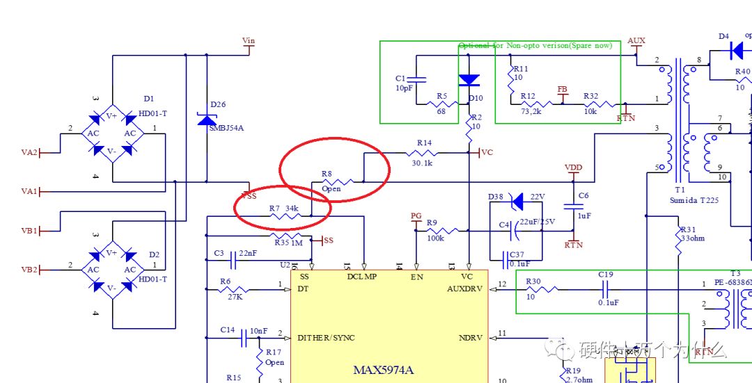
The SS pin is the soft-start programming capacitor connection. Connect a capacitor between SS and GND to set the soft-start period. This capacitor also determines the restart time of the hiccup mode current limit. The resistance between SS and GND can also be used to set DMAX below 75%. Connect a capacitor CSS between SS and GND to set the soft start time. VSS controls the duty cycle of the oscillator during startup, so that the duty cycle increases slowly and smoothly to its steady-state value. Calculate the CSS value as follows:
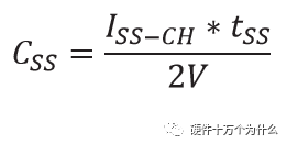
Among them, ISS-CH (10μA, typical value) is the CSS charging current during soft start, and tSS is the set soft start time. By connecting a resistor between SS and ground, the voltage on SS can be set lower than 2V. VSS is calculated as follows:

The power supply of this module chooses capacitance C3=22nF, and resistance R35=1MW.
3.3 Selection of transformer and switch tube
The success of the flyback transformer design depends largely on the quality of the transformer design. Different circuit topologies have different calculation formulas, but the transformers are basically designed based on the AP method. Some people who have extensive experience in power supply can often design a good transformer without too much calculation. The transformer parameters calculated by the formula are often only the transformer turns ratio, wire diameter, transformer core and transformer skeleton, etc. If you want to design a good transformer, only these are not enough, but also consider the winding method of the transformer and how the transformer is wound. An important parameter. Because the final performance of the transformer obtained by different transformer winding methods is very different, for example, the transformer with sandwich winding method has lower leakage inductance. Anyway, there are too many things to consider in the design of the transformer. If the performance of the transformer is poor, you can adjust the number of turns, change the winding method or change a transformer core.
This module uses the purchased transformer Sumida T225, because the switching frequency of this module is higher, and the transformer size is also required. After many discussions, it was decided to buy the transformer instead of winding it by itself. The performance of this transformer is found to be very good through testing, no abnormality occurs when the transformer is heavily loaded, and the output voltage is also normal.
The switch tube selection of the flyback switching power supply must satisfy that the drain source can withstand the input voltage plus 1.5 times the voltage coupled by the secondary side of the transformer to ensure that the switch tube will not be broken down when it is turned off. The leakage source of the switching tube must be able to flow twice the input current to ensure that the switching tube will not be damaged due to overcurrent. The loss of the switching tube occupies a certain proportion in the loss of the entire power module. Generally, MOSFETs with short rise and fall times of the switching tube are selected to ensure that the voltage and current overlap during a period of time when the switching tube is turned on and off. Loss.
4Power PDN and ripple noise
4.1 Power PDN
The power supply ripple noise test is a more complicated test problem. The results measured by different methods are different, even if the same test method is different, the test results of different people will generally be different.
For terminal products, whether it is CPU, GPU, DDR, etc., there are thousands of transistors inside the chip, and different circuits in the chip require different power supplies, such as Vcore, Vcpu, Vmem, VIO, Vgpu, Vpll Etc., these power supplies are powered by DC-DC power modules and LDO power modules, all managed by PMU.
As shown in Figure 4, it is the PDN diagram of the chip. The power supply loop of the chip starts from the voltage regulator module VRM, goes to the power supply network of the PCB, the ball pin of the chip, the power supply network of the chip package, and finally reaches the die. When the chip is working Under different loads, the VRM cannot respond to the load's demand for rapid changes in current in real time, resulting in a drop in the chip power supply voltage, resulting in power supply noise. For the VRM of the switching power supply module, the power supply itself will generate a power supply ripple consistent with the switching frequency, which is always superimposed on the power supply for output. For power supply noise, it is necessary to use decoupling capacitors on the package and PCB, design a reasonable power ground plane, and finally filter the power supply noise. For power supply ripple, it is necessary to increase the BULK inductor or BULK capacitor.
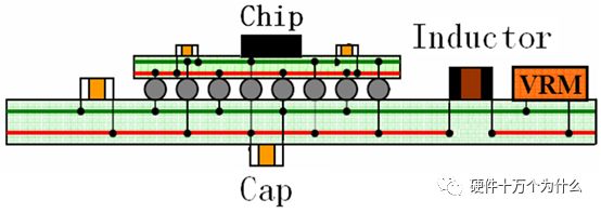
Figure 4 Schematic diagram of chip power distribution network (PDN)
For board-level PCB design, when the frequency reaches a certain frequency, due to the influence of the ESL of the trace and the ESL of the capacitor, high-frequency noise can no longer be filtered out. The industry believes that PCB can only handle noise within 100MHz, and higher frequency noise is required Package or die to solve. Therefore, for board-level power supply noise testing, an oscilloscope with a bandwidth of 500M or more is sufficient. In general, the larger the bandwidth of the oscilloscope, the higher the low noise. Therefore, it is recommended to limit the bandwidth of the oscilloscope to 1GHz when testing the power supply.
4.2 Power supply ripple and power supply noise

Figure 5 Power ripple and noise diagram
When measuring power supply ripple, limit the bandwidth of the oscilloscope to 20MHz, and measure the peak-to-peak value of the waveform output by the PMU power supply. After the design of the PMU chip is completed, the chip manufacturer will do a load test to test the ripple of the PMU output power under different loads. Therefore, there is no need to do this test on the terminal product board. The ripple size refers to the PMU. The manual is fine.
When testing the power supply noise, the test point is placed on the SINK terminal. Since the working speed of the SINK terminal is mostly above tens of MHz, the oscilloscope bandwidth is set to the full frequency band (the highest is the upper limit of the oscilloscope bandwidth), and the test point should be as close as possible to the power pin of the test chip , If there are multiple power pins, the pin farthest from the PMU should be selected. The power supply noise is related to the PCB layout and the position of the DECAP capacitor. At the same time, the power supply noise affects the working state of the CPU and the EMI of the single board. The terminal product board needs to test the power noise of each single board.
5Common Ripple and Noise Test Schemes
5.1 Basic requirements for ripple and noise testing
ç›®å‰èŠ¯ç‰‡çš„工作频率越æ¥è¶Šé«˜ï¼Œå·¥ä½œç”µåŽ‹è¶Šæ¥è¶Šä½Žï¼Œå·¥ä½œç”µæµè¶Šæ¥è¶Šå¤§ï¼Œå™ªå£°è¦æ±‚ä¹Ÿæ›´åŠ è‹›åˆ»ï¼Œä»¥MSM8974çš„COREæ ¸ä¸ºä¾‹ï¼Œç”µåŽ‹ä¸º0.9V,电æµä¸º3A,è¦æ±‚25MHz时,交æµPDN阻抗为22mohm,电æºå™ªå£°è¦æ±‚在±33mV以内。对于DDR3芯片,è¦æ±‚VREF电æºå™ªå£°åœ¨Â±1%以内,若1.5V供电,则噪声峰峰值ä¸å¤§äºŽ30mV。

这类低噪声的电æºæµ‹è¯•éžå¸¸å…·æœ‰æŒ‘战,影å“其测é‡å‡†ç¡®æ€§çš„主è¦æœ‰å¦‚ä¸‹å‡ ç‚¹ï¼š
(1)示波器通é“的底噪;
(2)示波器的分辨率(示波器的ADCä½æ•°ï¼‰ï¼›
(3)示波器垂直刻度最å°å€¼ï¼ˆé‡åŒ–误差);
(4)探头带宽;
(5)探头GND和信å·ä¸¤ä¸ªæµ‹è¯•ç‚¹çš„è·ç¦»ï¼›
(6)示波器通é“的设置;
在测试电æºå™ªå£°æ—¶ï¼Œè¦æ±‚如下æ¡ä»¶ï¼š
(1)需è¦åœ¨é‡è´Ÿè½½æƒ…况下测试电æºçº¹æ³¢ï¼›
(2)测试电æºçº¹æ³¢æ—¶åº”该将CPUã€GPUã€DDR频率é”定在最高频;
(3)测试点应该在SINK端è·ç¦»PMU最远的ä½ç½®ï¼›
(4)测试点应该é 近芯片的BALLï¼›
(5)带宽设置为全频段;
(6)示波器带宽大于500MHz;
(7)噪声波形å 整个å±å¹•çš„2/3以上或者垂直刻度已ç»ä¸ºæœ€å°å€¼ï¼›
(8)探头地和信å·ä¹‹é—´çš„回路最çŸï¼Œç”µæ„Ÿæœ€å°ï¼›
(9)测试时间大于1minï¼Œé‡‡æ ·æ—¶é—´1msä»¥ä¸Šï¼Œé‡‡æ ·çŽ‡500Ms/s以上;
(10)纹波噪声看Pk-Pk值,关注Maxã€Min值;
5.2高通滤波器特性分æž
示波器有ACå’ŒDC两ç§è€¦åˆæ–¹å¼ï¼Œå½“采用AC耦åˆæ—¶ï¼Œå…¶å†…部ç‰æ•ˆç”µè·¯å¦‚图6所示,C为隔值电容,R为终端对地阻抗,Vi为输入信å·ï¼ŒVo为测é‡ä¿¡å·ï¼Œæ»¤æ³¢å™¨çš„截æ¢é¢‘率为

 为信å·é¢‘率,则有:

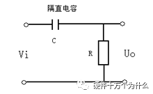
图6åŠ éš”å€¼ç”µå®¹åŽé«˜é€šæ»¤æ³¢å™¨ç‰æ•ˆç”µè·¯
表3 ä¸åŒéš”值电容对应的频点
| 隔直电容容值(uF) | 50W截æ¢é¢‘率(KHz) | 50W-1%误差频点(KHz) | 50W截æ¢é¢‘率(Hz) | 1MW-1%误差频点(Hz) |
| 0.1 | 31.83 | 222.82 | 1.5915 | 11.14 |
| 0.47 | 6.77 | 47.41 | 0.3386 | 2.37 |
| 1 | 3.18 | 22.28 | 0.1592 | 1.11 |
| 2.2 | 1.45 | 10.13 | 0.0723 | 0.51 |
| 10 | 0.32 | 2.23 | 0.0159 | 0.11 |
5.3æ— æºæŽ¢å¤´DC耦åˆæµ‹è¯•
ä½¿ç”¨æ— æºæŽ¢å¤´DC耦åˆæµ‹è¯•ï¼Œç¤ºæ³¢å™¨å†…部设置为DC耦åˆï¼Œè€¦åˆé˜»æŠ—为1Mohm,æ¤æ—¶æ— æºæŽ¢å¤´çš„地线接主æ¿åœ°ï¼Œä¿¡å·çº¿æŽ¥å¾…测电æºä¿¡å·ã€‚è¿™ç§æµ‹é‡æ–¹æ³•å¯ä»¥æµ‹åˆ°é™¤DC以外的电æºå™ªå£°çº¹æ³¢ã€‚
如图7所示,当采用普通的鳄鱼夹探头时,由于地和待测信å·ä¹‹é—´çš„环路太大,而探头探测点é 近高速è¿è¡Œçš„IC芯片,近场è¾å°„较大,会有很多EMI噪声è¾å°„到探头回路ä¸ï¼Œä½¿æµ‹è¯•çš„æ•°æ®ä¸å‡†ç¡®ã€‚为了改善这ç§æƒ…况,推èç”¨æ— æºæŽ¢å¤´æµ‹è¯•çº¹æ³¢æ—¶ï¼Œä½¿ç”¨å³å›¾ä¸çš„探头,将地信å·ç¼ 绕在信å·å¼•è„šä¸Šï¼Œç›¸å½“于在地和信å·ä¹‹é—´å˜åœ¨ä¸€ä¸ªçŽ¯è·¯ç”µæ„Ÿï¼Œå¯¹é«˜é¢‘ä¿¡å·ç›¸å½“于高阻,有效抑制由于è¾å°„产生的高频噪声。更多时候,建议测试者采用第三ç§æµ‹è¯•æ–¹æ³•ï¼Œå°†ä¸€ä¸ªæ¼†åŒ…线绕在探头上,然åŽå°†æ¼†åŒ…线的焊接到主æ¿åœ°ç½‘络上,移动探头去测试æ¯ä¸€è·¯ç”µæºçº¹æ³¢å™ªå£°ã€‚åŒæ—¶æ— æºæŽ¢å¤´è¦æ±‚å°½é‡é‡‡ç”¨1:1的探头,æœç»ä½¿ç”¨1:10的探头。

图7 æ— æºæŽ¢å¤´åœ°çº¿ä¸¤ç§å¤„ç†æ–¹æ³•
对于示波器,若垂直刻度为xV/div,示波器垂直方å‘为10div,满é‡ç¨‹ä¸º10xVï¼Œç¤ºæ³¢å™¨é‡‡æ ·AD为8ä½ï¼Œåˆ™é‡åŒ–误差为10x/256 V。例如一个1V电æºï¼Œå™ªå£°çº¹æ³¢ä¸º50mV,如果è¦æ˜¾ç¤ºè¿™ä¸ªä¿¡å·ï¼Œéœ€è¦è®¾ç½®åž‚直刻度为200mV/div,æ¤æ—¶é‡åŒ–误差为7.8mV,如果把直æµ1V通过offset去掉,åªæ˜¾ç¤ºçº¹æ³¢å™ªå£°ä¿¡å·ï¼Œåž‚直刻度设置为10mVå³å¯ï¼Œæ¤æ—¶çš„é‡åŒ–误差为0.4mV。
ä½¿ç”¨æ— æºæŽ¢å¤´DC耦åˆæµ‹è¯•ï¼Œç¤ºæ³¢å™¨è®¾ç½®å¦‚下:
(1)1Mohm端接匹é…ï¼›
(2)DC耦åˆï¼›
(3)全带宽;
(4)offset设置为电æºç”µåŽ‹ï¼›
5.4æ— æºæŽ¢å¤´AC耦åˆæµ‹è¯•
ä½¿ç”¨æ— æºæŽ¢å¤´DC耦åˆéœ€è¦è®¾ç½®offset,对于电æºç”µåŽ‹ä¸ç¨³å®šçš„情况,offset设置ä¸åˆç†ï¼Œä¼šå¯¼è‡´å±å¹•ä¸Šæ˜¾ç¤ºçš„ä¿¡å·è¶…出é‡ç¨‹ï¼Œæ¤æ—¶é€‰æ‹©AC耦åˆï¼Œä½¿ç”¨å†…置的æ置电路æ¥æ»¤åŽ»ç›´æµåˆ†é‡ã€‚对于大多数的示波器,会有如下å‚数,设置为AC耦åˆï¼Œæ¤æ—¶æµ‹é‡çš„为10Hz以上的噪声纹波。

图8 示波器两ç§è€¦åˆæ–¹å¼é¢‘点
ä½¿ç”¨æ— æºæŽ¢å¤´AC耦åˆæµ‹è¯•ï¼Œè®¾ç½®å¦‚下:
(1)1Mohm端接匹é…ï¼›
(2)AC耦åˆï¼›
(3)全带宽;
(4)offset设置为0
5.5åŒè½´çº¿å¤–部隔直电容DC50欧耦åˆæµ‹è¯•
ç”±äºŽæ— æºæŽ¢å¤´çš„带宽较低,而电æºå¼€å…³å™ªå£°ä¸€èˆ¬éƒ½åœ¨ç™¾MHz以上,åŒæ—¶ç”µæºå†…é˜»ä¸€èˆ¬åœ¨å‡ ç™¾æ¯«æ¬§ä»¥å†…ï¼Œé€‰æ‹©é«˜é˜»1Mohmçš„æ— æºæŽ¢å¤´å¯¹äºŽé«˜é¢‘会产生åå°„çŽ°è±¡ï¼Œå› æ¤å¯ä»¥é€‰æ‹©ç”¨åŒè½´çº¿æ¥ä»£æ›¿æ— æºæŽ¢å¤´ï¼Œæ¤æ—¶ç¤ºæ³¢å™¨ç«¯æŽ¥é˜»æŠ—设置为50欧,与åŒè½´çº¿é˜»æŠ—相匹é…ï¼Œæ ¹æ®ä¼ 输线ç†è®ºï¼Œç”µæºå™ªå£°æ²¡æœ‰å射,æ¤æ—¶è®¤ä¸ºæµ‹é‡ç»“果最准确。
利用åŒè½´çº¿çš„测é‡æ–¹æ³•ï¼Œæœ€å‡†ç¡®çš„是采用DC50欧,但是大部分示波器在DC50欧时offset最大电压为1Vï¼Œæ— æ³•æ»¡è¶³å¤§éƒ¨åˆ†ç”µæºçš„测é‡è¦æ±‚,而示波器内部端接阻抗为50欧时,ä¸æ”¯æŒAC耦åˆï¼Œå› æ¤éœ€è¦å¤–置一个AC电容,如图9所示,当串è”电容值为10uFæ—¶ï¼Œæ ¹æ®è¡¨3å¯ä»¥çœ‹åˆ°ï¼Œæ¤æ—¶å¯ä»¥å‡†ç¡®æµ‹è¯•åˆ°2KHz以上的纹波噪声信å·ã€‚
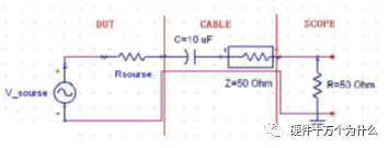
图9 åŒè½´çº¿DC50测é‡å›¾
5.6åŒè½´çº¿AC1M欧耦åˆæµ‹è¯•
由于从PMU出æ¥çš„电æºçº¹æ³¢å™ªå£°å¤§å¤šé›†ä¸åœ¨1MHz以内,如果采用åŒè½´çº¿DC50外置隔直电容测é‡æ–¹æ³•ï¼Œä½Žé¢‘噪声分é‡æŸå¤±è¾ƒä¸ºä¸¥é‡ï¼Œå› æ¤æ”¹ç”¨å›¾10所示的测é‡æ–¹æ³•ï¼Œåˆ©ç”¨åŒè½´çº¿ä¼ 输信å·ï¼Œç¤ºæ³¢å™¨è®¾ç½®ä¸ºAC1Mï¼Œè¿™æ ·è™½ç„¶å˜åœ¨å射,但是åå°„ä¿¡å·ç»è¿‡è¾ƒé•¿CABLEçº¿æŠ˜è¿”ä¼ è¾“åŽï¼Œå½±å“是有é™çš„,示波器在R2上采集电压值å¯ä»¥è®¤ä¸ºä»ç„¶å¯ä»¥è¢«å‚考。
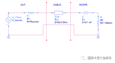
图10 åŒè½´çº¿AC1M测é‡å›¾
为了é¿å…å射,在åŒè½´çº¿æŽ¥åˆ°ç¤ºæ³¢å™¨çš„接å£å¤„端接一个50ohm电阻,使示波器输入阻抗和cable线特å¾é˜»æŠ—匹é…。
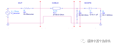
图11 åŒè½´çº¿AC1M测é‡æ”¹è¿›å›¾
5.7差分探头外置电容DC耦åˆæµ‹è¯•
由于示波器的探头地和机壳地通过一个å°ç”µå®¹æŽ¥åœ¨ä¸€èµ·ï¼Œè€Œç¤ºæ³¢å™¨çš„机壳地åˆé€šè¿‡ä¸‰è§’æ’å¤´å’Œå¤§åœ°æŽ¥åœ¨ä¸€èµ·ï¼Œåœ¨å®žéªŒå®¤é‡Œï¼Œå‡ ä¹Žæ‰€æœ‰çš„è®¾å¤‡åœ°éƒ½å’Œå¤§åœ°æŽ¥åœ¨ä¸€èµ·ï¼Œç¤ºæ³¢å™¨å†…éƒ¨åœ°çº¿æŽ¥æ³•å¦‚å›¾12æ‰€ç¤ºï¼Œå› æ¤ä¸Šé¢ä»‹ç»çš„两ç§æ–¹æ³•éƒ½æ— 法解决地干扰问题,为了解决这个问题,需è¦å¼•å…¥æµ®åœ°ç¤ºæ³¢å™¨æˆ–者差分探头。
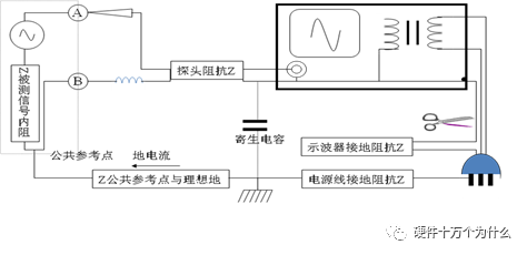
图12示波器内部地线接法
如图13所示,为差分接法,由于差分探头为有æºæŽ¢å¤´ï¼Œå¤–置差动放大器,å¯ä»¥å°†å¾…测信å·é€šè¿‡å·®åˆ†æ–¹å¼æŽ¥å…¥ï¼Œä½¿ç¤ºæ³¢å™¨çš„地和待测件地隔离开,达到浮地效果。但是差分探头在示波器内部åªèƒ½DC50欧耦åˆï¼Œè€Œoffset最大一般ä¸è¶…过1Vï¼Œå› æ¤éœ€è¦åœ¨å·®åˆ†æŽ¢å¤´ä¸Šä¸²è”隔直电容。使用差分探头测é‡æ—¶å…³é”®æ˜¯æŽ¢å¤´çš„CMRRè¦è¶³å¤Ÿå¤§ï¼Œè¿™æ ·æ‰èƒ½æœ‰æ•ˆæŠ‘制共模噪声
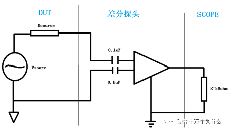
图13差分探头外置电容DC耦åˆæŽ¥æ³•ç¤ºæ„图
5.8差分探头衰å‡DC耦åˆæµ‹è¯•
当采用差分探头外置电容DC耦åˆæ—¶ï¼ŒåŒæ ·å˜åœ¨æˆªæ¢é¢‘率的问题,测é‡çš„结果会æŸå¤±ä¸€äº›ä½Žé¢‘分é‡ï¼Œä¸ºäº†è§£å†³è¿™ä¸ªé—®é¢˜ï¼Œå¯ä»¥å°†å·®åˆ†æŽ¢å¤´è¡°å‡10å€ï¼Œç¤ºæ³¢å™¨ä¼šå°†é‡‡é›†åˆ°çš„电压值乘10显示出æ¥ï¼Œè¿™ä¸ªæ—¶å€™offset设置也会放大到10V,能够满足终端类产å“çš„ç›´æµç”µåŽ‹å置。
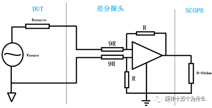
图14 差分探头衰å‡DC耦åˆæµ‹è¯•æŽ¥æ³•ç¤ºæ„图
6电æºæ¨¡å—电压测试
由于本模å—是POE电æºï¼Œæµ‹è¯•æ‰€ä½¿ç”¨çš„输入电压å–自于网å£ï¼ŒPSE供电模å—会和本模å—先进行æ¡æ‰‹é€šä¿¡ï¼ŒPSE设备确定åŽé¢æ‰€æŽ¥çš„是PD设备åŽï¼Œæ‰ç»™PD设备供电。如图15所示为一个PoE SWITCH设备。
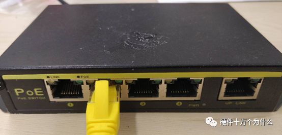
图15 PoE SWITCH设备
如图16所示为本模å—电路,电路长大约6.2cm,宽大约2.65cm,高大约1.5cm。
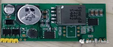
图16 POE电æºæ¨¡å—
由于给POE电æºæ˜¯é€šè¿‡ç½‘å£ä¾›ç”µçš„,本模å—没有特别设计一个网络端å£æ¥ç»™ä¾›ç”µï¼Œè€Œæ˜¯ä½¿ç”¨â€œç¡¬ä»¶å万个为什么â€æ供的开å‘æ¿ï¼Œæ¤å¼€å‘æ¿æ˜¯ç”¨æ¥ç»™ç‰©è”网编程用的,属于工业兼å¦ä¹ 使用的一å—å¼€å‘æ¿ï¼Œå¯ä»¥ä½¿ç”¨å¼€å‘æ¿æ¥å®žçŽ°wifiã€GPRSã€è“牙ã€ä¸²å£ã€LORAã€POEç‰åŠŸèƒ½çš„使用,故直接选择æ¤å—å¼€å‘æ¿æ¥å®žçŽ°ç½‘络端å£ä¾›ç”µã€‚如图17所示为网络供电端å£ã€‚
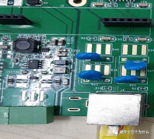
图17 网络端å£ä¾›ç”µæ¨¡å—
6.1输入电压测é‡
图18所示为通过网络端å£è¿‡åŽåœ¨POE电æºè¾“入端å£æµ‹çš„电压,æ¤æ¬¡æ‰€ä½¿ç”¨çš„示波器是鼎阳牌SDS1000X-Cæ•°å—示波器。
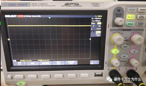
图18 输入电压波形
输入电压也有一定的纹波,图19所示就是输入电压的纹波,å¯ä»¥çœ‹å‡ºçº¹æ³¢è¿˜æ˜¯æ¯”较å°çš„,是å¯ä»¥æŽ¥å—的纹波范围。
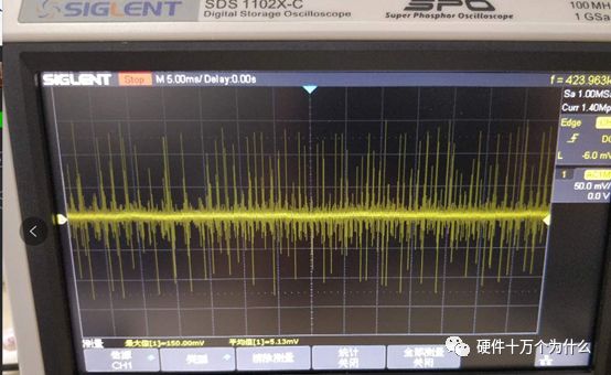
图19 输入电压纹波测试
6.2输出电压测é‡
本模å—输出电压应该是5V输出,但是由于很难把电压一直稳定在5Vä¸å˜ã€‚
图20所示就是输出电压测试,从万用表ä¸çœ‹å‡ºï¼Œè¾“出电压在5.1V。
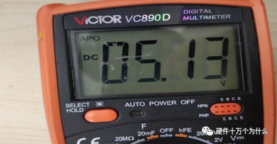
图20 输出电压测试
输出电压也是有纹波的,图21所示就是输出电压的纹波测试图。
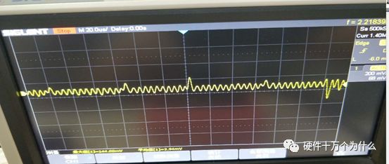
图21 输出电压纹波
从输出纹波å¯ä»¥çœ‹å‡ºï¼Œæ¤çº¹æ³¢åœ¨å¯æŽ¥å—范围内的。
7总结
本文档简è¦ä»‹ç»äº†POE电æºçš„基础知识,以åŠæ•´å—电路芯片以åŠå…ƒä»¶é€‰åž‹ï¼Œç”µè·¯åŽŸç†çš„介ç»ã€‚电æºçº¹æ³¢çš„产生以åŠæµ‹è¯•æ–¹æ³•çš„介ç»,POE电æºçš„测试设备介ç»ï¼Œä»¥åŠè¾“入输出电压的测é‡ç‰ã€‚
Customized Engineering Ceramics
Customized Engineering Ceramics,Ceramic Plate,Machinery Ceramic Part,Metalized Ceramic Base
Yixing Guangming Special Ceramics Co.,Ltd , https://www.yxgmtc.com