To minimize power consumption, a simple MOSFET is typically used to power unused circuits. However, a better option is to use a load switch because it has extra features to handle many of the subtle and unpredictable problems of power rail management.
The load switch provides a range of performance parameters and ratings from multiple suppliers, which allows for a good fit between the application priority and the available components.
This article will briefly discuss IC and circuit shutdown concepts, then introduce the appropriate load switch options and how to use them.
Power down optionMinimizing power consumption by temporarily turning off unneeded functions is a standard system strategy. For this reason, many ICs have a user-oriented ultra-low power static mode.
However, placing the IC in static mode only turns off the IC rather than the associated circuitry, including other power-dissipating passive components (primarily resistors) and active discrete components such as transistors. As a result, designers often turn to simple MOSFETs to turn off the power to the entire subsection.
This MOSFET may be required even if the power supply (LDO or switch) can be turned off by enabling the control line to reduce the idle mode power consumption of its load subcircuit. The reason is that although the savings may be large, even in the shutdown mode, many power supplies have relatively large leakage currents, so power saving may not be sufficient.
While it is possible to use appropriately sized MOSFETs as power rail switchers, MOSFETs offer few features and functions, and often do not support other on/off switching requirements. In addition, circuit designers must provide the appropriate gate drivers for the MOSFETs, which becomes another item in the “to do†list, thus increasing design complexity, time, space, and cost.
Load switches provide an "integrated" solutionA better approach is to use a “load switch†IC, which is a pass-through MOSFET and adds additional power management features in a small package. Most load switches have only 4 pins, one for each input voltage, output voltage, logic level enable and ground (Figure 1).

Figure 1: The base load is a four-terminal device that combines MOSFET and MOSFET drivers in an easy-to-use package. (Source: Texas Instruments )
The operation is very simple: when the load switch is enabled through the ON pin, the pass FET turns on and allows current to flow from the input (source) voltage pin to the output (load) voltage pin. Like the basic MOSFET, the DC resistance through the "switch" is only a few milliohms (mΩ), so the voltage is reduced and the associated power dissipation is also the same.
The load switch is more than just a MOSFET and a driver that can be turned on/off with a simple logic level signal. Although using this feature alone may make the load switch better than a MOSFET with a separate driver, the load switch has more features (Figure 2).
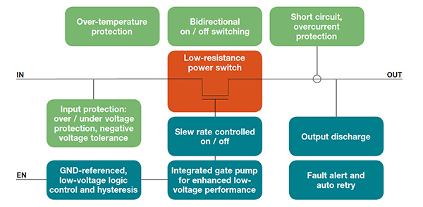
Figure 2: Load switches typically have other functions, including discharge control, slew rate control, various forms of protection, and fault monitoring. (Source: Vishay Siliconix )
In addition to the logic level control function, why use a load switch? There are several reasons:
The overall driver manages the charging and discharging of the gates to provide slew rate control of the MOSFET turn-on/turn-off cycle rise/fall times. This optimizes MOSFET performance, avoids overshoot and ringing, and minimizes undesirable EMI / RFI.
In addition, by controlling the on-time of the MOSFET in the switch, it is possible to prevent the input voltage rail from sagging due to a sudden increase in the inrush current caused by a quick attempt to charge the load capacitor. This issue can be problematic if the same input rails are also supplying power to other subsystems that must be fully powered.
Some load switches provide fast output discharge (QOD) through an on-chip resistor between the output and ground; Â This mode is activated when the device is disabled by the ON pin. This will discharge the output node and prevent the output from floating, which can cause unwanted activity when the load circuit is not turned off to a defined state.
Note that this feature is sometimes unpopular: if the output of the load switch is connected to the battery, this fast output discharge can cause the battery to run out when the load switch is disabled via the ON pin - this is not a good thing! Therefore, some vendors offer it as an optional feature in a single device, while others offer variants of two load switches, one with it and the other without. The former option allows multiple identical components to be used for a single product, but is used in different situations.
The load switch can include other functions such as thermal shutdown, undervoltage lockout, current limit and reverse current protection, all of which can be used on power supplies and rails. These protection features contribute to system level integrity.
Overall BOM, design time and real estate costs can be significantly reduced compared to starting to use basic MOSFETs to switch power rails and add these features.
Further, the use of load switches is not limited to simple shutdown to save power. By using a set of load switches, a single larger power supply can power multiple circuit sub-portions whose up/down power is achieved by a defined sequence and timing under multiple digital output controls (Figure 3). In this way, the load switch acts as a gating component for a broader and more efficient power management control scheme.
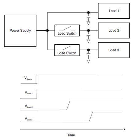
Figure 3: The load switch allows multiple loads to drive multiple loads, each with independent on/off and relative timing. (Source: Texas Instruments)
Keep in mind that the load switch requires a capacitor (usually 1 microfarad (μF)) on its input side to limit the input supply voltage drop caused by the transient inrush current flowing into the discharge load capacitor. They also need to "see" a load capacitor that is about one tenth of the input capacitance value;  If the load is less than this value, a small output capacitor should be added.
Load switch parametersThe performance properties of the load switch begin with a standard FET that acts as an on/off switch. These include:
On resistance (R  On ) determines the voltage drop across the load switch and the power consumption of the switch. Typical values ​​are in the tens of milliohms range, but vary with individual supplier products and load switch current capacity. The designer must do some basic calculations to determine the maximum allowable value in the application.
Maximum voltage (V  In ) and current (I  The max ) rating specifies how high the switch can withstand and how large the maximum current is. Designers should check steady state values ​​and the transients and peaks of these factors.
Other parameters are quiescent current and shutdown current. The quiescent current is the current consumed by the load switch when the load switch is turned on, and thus becomes a waste of power. This is negligible compared to the power consumed by the load itself. The shutdown current is the current that "leaks" from the load switch to the load when the switch is in the shutdown mode.
Load switching from simple to complexA good example of a load switch with additional features is the NCP330 from ON Semiconductor . This is a basic N-channel MOSFET load switch, but it includes a 2 millisecond soft-start mode for applications where sudden load applications can be harmful. This is usually necessary in mobile applications with limited battery capacity (Figure 4).
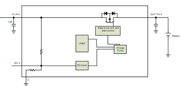
Figure 4: ON Semiconductor's NCP330 load switch includes a 2 millisecond swing mode so the load is not suddenly connected to the power supply. This prevents various operational and performance issues with supply and load. (Source: ON Semiconductor)
The NCP330's very low on-resistance, only 30mΩ, makes it ideal for system batteries that charge at 3 amps (A). If the power supply is connected to the Vin pin (active high), the 1.8 V to 5.5 V device will be automatically enabled. If there is no input voltage, it remains off through an internal pull-down resistor. Reverse voltage protection is also built in.
Vishay Siliconix offers SiP32408 and SiP32409 slew rate control load switches (2.5 V 3.6 V) designed for operation from 1.1 V to 5.5 V. The SIP32409 is identical to the SiP32408 but has a fast turn-off output discharge circuit. One of the key features is that its on-resistance (typically 42mΩ) remains flat over most of the 1.5 to 5 volt supply range. Another property is that the control enable voltage is also low, so it can be used in low voltage circuits without the need for a level shifter (Figure 5).
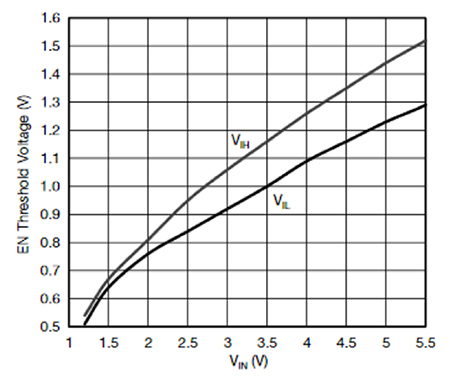
Figure 5: The relationship between the control enable signal low and high logic level thresholds and the input voltage for the SiP32408 and similar SiP32409 load switches from Vishay Siliconix. (Source: Vishay Siliconix)
Although load switches are relatively simple devices in terms of the number and function of package pins, layout is still a problem when current flows and possible parasitics. For this reason, it is best to use the company's recommended printed circuit board layout (Figure 6) and the top and bottom layout of the 1 x 1 inch (2.5 x 2.5 cm) evaluation board (Figure 7).
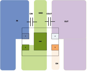
Figure 6: The printed circuit board layout and component layout needs to be carefully planned to achieve the full performance of the load switches (such as the SiP32408 and SiP32409) so that ground noise, parasitics, and current do not affect maximum performance. (Source: Vishay Siliconix)
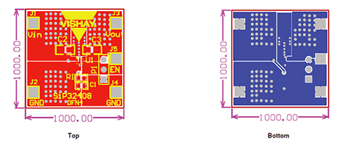
Figure 7: In addition to showing the preferred printed circuit board layout for the SiP32408 and SiP32409, Vishay Siliconix also provides a layout for the small evaluation boards for these devices. (Source: Vishay Siliconix)
The load switch used at the increasingly common lower voltage is Texas Instruments (Texas Instruments)  The TPS22970 can operate from input voltages as low as 0.65 V to 3.6 V (Figure 8). The on-resistance is also very low, typically 4.7mΩ from a 1.8V input and slightly up to 6.4mΩ at 0.65V. The switch handles 4 A of continuous current with an on-state quiescent current of 30μA (typ) input voltage of 1.2 V and an off-state current of 1μA at input voltages above 1.8 V.

Figure 8: The basic application of the TPS22970 shows critical input (source) capacitance and sometimes unnecessary output (load) capacitance; Â It also clearly shows that the load switch is a simple four-terminal device. (Source: Texas Instruments)
The TPS22970 features an on-chip resistance of 150Ω to quickly discharge the output when the switch is disabled. This avoids any unknown state caused by the load seeing the floating power supply. When the input voltage is 3.6 volts and 0.65 volts, respectively, the turn-on rate control turn-on time is 1.5 milliseconds (ms) and 0.8 milliseconds, respectively. A comprehensive data sheet (up to 25 pages for four-terminal equipment) contains many detailed tables and charts that can be fully characterized from a variety of perspectives. For example, it shows the rise and fall times of each of the four input voltages versus temperature (Figure 9).

Figure 9: The load resistance of the TPS22970 is 10Ω, and the rise time (left) and fall time (right) of the load capacitance at 0.1μF are related to temperature. (Source: Texas Instruments)
in conclusionThe MOSFET itself provides a simple solution to turn the DC on and off to minimize power consumption, achieve sequencing of multiple loads, and control power sequencing. However, load switches that integrate MOSFETs, drivers, slew rate control, and various forms of fault protection are generally better choices because they provide all of these additional features in a single small form factor device.
Load switches provide a range of performance parameters and ratings from multiple suppliers that are well adapted to application priorities and available components.
Eye protection:The principle of chlorophyll defocusing is adopted to prevent the eyeball from focusing for a long time, effectively alleviate eye fatigue, and achieve better eyesight protection.
Anti-blue light, ultraviolet light:The Green Light Film can actively filter the target wavelength while providing a band in the range of 380-400nm. It can effectively block 100% harmful light.
Edge coverage:The soft material fully covers the edges of any device, so it can be affixed to curved screen and round edges, 100% provides excellent edge coverage, and there is no gap between the edges of the device.
Oleophobic and waterproof:The oleophobic coating surface of the Green Light Screen Protector can provide your phone with oleophobic and waterproof properties, which can prevent sweat, grease residue, and fingerprints.
Sensitive touch:The 0.14mm ultra-thin film does not interfere with the touch response, almost as if it does not exist. When using a mobile phone, the fingertips can be easily swiped, bringing you a comfortable gaming experience.
Green Light Film,Green Light Screen Protector,Anti Green Light Screen Protector,Anti-green Light Screen Protector
Shenzhen Jianjiantong Technology Co., Ltd. , https://www.jjtscreenprotector.com