According to a report by Mames Consulting, researchers from Yale University and the Barcelona Institute of Photonics (ICFO) have jointly developed a graphene-based device, or can be made into a new micro-size that works in the mid-infrared spectrum. Uncooled detector.
At present, commercial mid-infrared sensors that work in the infrared "fingerprint" area (full of molecular-specific spectral information) usually require expensive photodetector materials and also require cooling of the system, which makes the instrument very bulky.
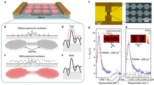
The working wavelength of the sensor developed by the Yale-ICFO cooperative team is located at 12.2 um at the core of the mid-infrared spectrum and is composed of a plasma resonator array. The size of the device is only 5um x 5um, and it has good low-noise performance at room temperature without any cooling.
"This device is made of large-scale graphene and has a simple two-terminal geometry. It represents an important step in the realization of an on-chip graphene mid-infrared detector array," the collaboration led by ICFO's Javier Garcia de Abajo and Yale University's Fengnian Xia The project, in a paper just published in "Nature Materials" (Nature Materials) magazine, introduced the research results in detail.
Gigahertz speedICFO researchers claim that they can greatly improve the sensitivity of the device by using the resonant coupling between mid-infrared light and graphene plasma.

The team fabricated sensors on graphene wafers, in which disc-shaped plasmonic resonators were interconnected by so-called "quasi-one-dimensional graphene nanoribbons."
When they illuminated the device with a mid-infrared light source, they observed the excitation and absorption of the infrared plasma on the surface of the graphene resonator and nanoribbons at room temperature.
Thanks to the graphene nanostructures, they also observed that the light absorption converted into electrical response is closely related to the plasma absorption level, and the response time can be detected at gigahertz speeds.
In the conclusion, the research team said: “The results of this study prove that graphene is an excellent material for ultra-fast conversion of optical signals into electrical signals at room temperature, which has promoted the development of ultra-small detectors and can integrate them into high High-resolution mid-infrared cameras or high-density integrated infrared photonic circuits."
Mid-infrared applicationsIf the technology can develop as expected, its application prospects should be very broad, and it may be a breakthrough. It can realize an ultra-compact device that recognizes based on molecular fingerprint vibration and rotation excitation.
The identifiable molecules will include dangerous goods and biomolecules. The ICFO team suggests that the technology can be applied to safety, biometrics, and air quality monitoring.
An application example of mid-infrared spectroscopy is carried on the James Webb Space Telescope (JWST), which is scheduled to be launched in 2020. JWST's "MIRI" instrument covers the 5-28 um spectral region and is used to study the red-shifted light from distant galaxies, newly formed stars and faint comets.

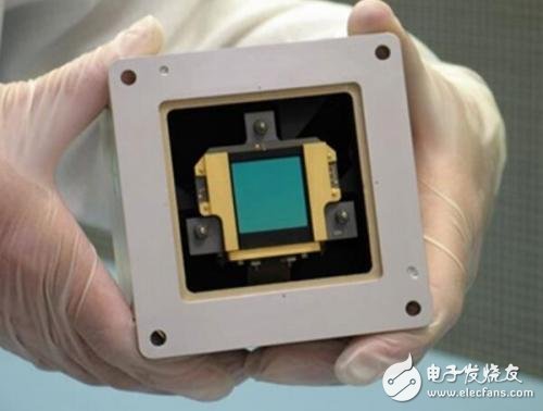
The MIRI detector is based on an arsenic-doped silicon sensor, manufactured by Raytheon Vision Systems. It has a complex low-temperature cooling device. The combination of a pulse tube precooler and a Joule-Thomson loop heat exchanger provides a temperature as low as 7 K.
Dongguan Guancheng Precision Plastic Manufacturing Co., Ltd. , https://www.dpowerchargers.com