In recent years, with the continuous narrowing of mainstream process line widths to below 90nm, and the increasing demand for the quality of digital audio playback, the audio processing module integrated within the SOC has slowly transformed into a single-chip solution. This puts higher demands on the power consumption, performance and function of the single-chip audio CODEC. Wuhan Guanghuaxin Technology Co., Ltd. designed low-power audio CODEC CJC8988 for mobile and portable applications, especially suitable for applications with low power consumption requirements such as wireless headphones, portable mp3, etc., where the power consumption of ADC is 1mW, and that of DAC The power consumption is 0.5mW. The chip has four microphone inputs and four headphone outputs. The chip uses a mature 0.18μ CMOS process with an operating voltage of 1.8V and low cost. The total power consumption of all channels of the entire chip is 9mW. The signal-to-noise ratio of the recording and playback channels is greater than 96db, and the total harmonic distortion is greater than 85dB.
1 CJC89888 chip features:
The chip supports two stereo inputs, either linear input or microphone input, single-ended input or differential input is optional, when using differential input can significantly improve the power supply suppression ratio to achieve better recording results. The use of an adjustable gain amplifier with automatic gain control can ensure a constant recording volume.
The chip supports multi-channel mixing to deal with complex application environments. The DAC playback and the mixing function of each analog channel ensure the flexible application of the chip.
On-chip 24bit ∑ △ ADC, DAC adopts multi-order oversampling ∑ △ architecture to ensure high performance and low power consumption requirements. The chip has digital audio processing functions, such as 3D sound enhancement function and frequency equalizer adjustment function. The principle of 3D sound effect enhancement is to use the principle of enhancing the difference between the left and right channels to achieve the effect of spatial stereoscopic enhancement. The frequency equalizer uses several different frequency response curves to achieve various sound effects.
The chip adopts the design of pop-up sound and the sequence of power-on configuration, which can make the influence of POP sound basically negligible.

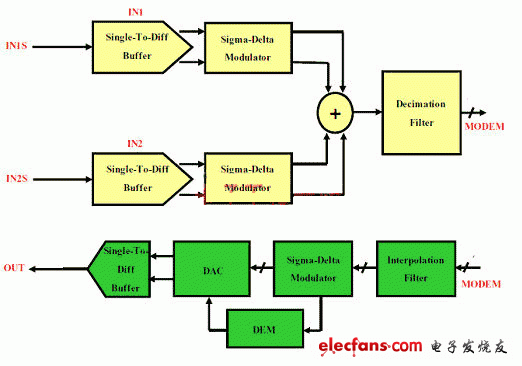
Figure 1: ∑ △ ADC & DAC block diagram
2 Low-power chip design points
In order to ensure low power consumption of the chip and no compromise in performance, it is necessary to carefully set the current ratio for each module of the chip.
Figure 1 is a simplified block diagram of audio processing. The single-ended signal is input to the modulator and decimation filter after a single-turn dual-drive amplifier and anti-aliasing filter to complete AD conversion. DA is a digital interpolation filter that reconstructs the filter and completes the analog-to-digital conversion.
The ADC uses a single-loop third-order multi-bit architecture. The single-loop architecture is insensitive to circuit mismatch and the limited bandwidth and gain of the op amp. It uses high-pass butterworth filter noise shaping and is simulated by simulink at 128 times oversampling rate Achieve 120bit signal-to-noise ratio. In the actual circuit implementation, the equivalent noise and KT / C noise of the first-stage op amp cannot be shaped by noise, so more area and power consumption need to be given to meet the signal-to-noise ratio and bandwidth requirements of the entire ADC .
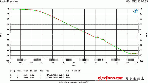
Using multi-bit quantizer can directly improve the performance of the modulator, but the error introduced by the multi-bit DAC in the feedback loop will reduce the performance of the modulator. Due to process errors, the actual value of each capacitor unit is somewhat different from the ideal value, and the actual output value of the DAC will be different from the ideal output value. This error will be the same as the input signal of this stage, without attenuating the output, and finally resulting in increased harmonics of the quantizer. Dynamic calibration and DWA (Data Weighted Averaging) are used here. The error of the DAC is represented as first-order noise shaping, and the process error of the DAC is moved to the high-frequency range, and filtered by the digital filter. The driver stage in front of the ADC performs both single-turn dual and anti-aliasing filtering functions. ClassAB two-stage op amps are used and the bias current must be carefully selected to ensure that crossover distortion is avoided and THD is guaranteed at the lowest possible bias current Harmonic distortion.

Figure 2: ADC THD + N raTIo vs input level with 1KHZ input
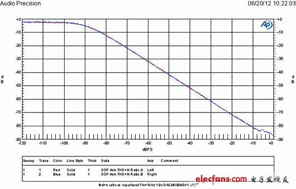
The DAC uses a third-order 4bit DSM modulator, SC filter and reconstruction filter to complete the digital-to-analog conversion. The DWA algorithm is still used here to suppress the capacitance process deviation. The input equivalent noise of the DAC must take into account KT / C noise and op amp noise. And thermal noise. The switch size of the SC filter should also take into account the linearity under the clock feed-through effect as small as possible. The test achieved a signal-to-noise ratio of 100dB and THD + N of 88dB, while the operating current of the DAC was less than 300μA.

Figure 3: DAC THD + N raTIo vs input level with 1KHZ input
For the various annoying POP sound problems of the audio chip, we use a combination of multiple methods. The first is the correct configuration sequence for power-on. At the same time, the output voltage of each channel and module should be kept at the common mode level as much as possible to reduce the impact caused by the level difference when each channel is switched. The volume adjustment needs to be adjusted at the time point when the sound signal crosses zero to reduce the impact sound, and the final effect can ensure the best customer experience of the audio chip.
The above are the brief design features of this low-power audio CODEC chip. While ensuring performance, the most optimized power consumption level can be obtained to meet the stringent requirements of low-power portable devices.
Mini LED Downlight includes round and square two shape frame. We are the manufacturer of producing energy saving interior lighting. This type of down light is made by PC material in frame and aluminum back cover. It has aluminum heat sinking and concealed mounted installation. There are three color temperatures with cool white, warm white and natural white of down lights. There are four colors Red/Blue/Green/Pink. The unique features of led downl light are: CRI>80, PF>0.5. These down lights LED are mainly apply to home, office and school and so on.
Mini LED Downlight
Commerial LED Downlight,Best LED Downlights,Sustainable Lighting Design
Jiangmen Lika Lighting Electrical Appliances Co., Ltd , https://www.lika-led.com