The so-called synthesis is to translate the design input of HDL language and schematic diagram into logical connection (netlist) of basic logic units such as AND, OR, NOT, RAM, and trigger, and optimize the target according to the target and requirements (constraints). Generated logical connections to generate EDF files. XST is embedded in versions of ISE 3 and is constantly being refined. In addition, because XST is Xilinx's own comprehensive tool, it has better integration for some of the unique structures of Xilinx chips.
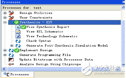
Once the input, simulation, and pin assignments are complete, they can be synthesized and implemented. Double-click Synthesize-XST in the process management area, as shown in Figure 5-1, to complete the synthesis and give initial resource consumption. Figure 5-2 shows the resources occupied by the module.

Figure 5-1 Design synthesis window

Figure 5-2 Comprehensive results report
There are three possible outcomes: if the synthesis is completely correct, there is a small green circle in front of the Synthesize-XST; if there is a warning, a small yellow circle with an exclamation mark appears; if there is an error, a band appears Red small circle of forks. After the integration is complete, you can view the RTL-level structure diagram by double-clicking View RTL SchemaTIcs to see if the integrated structure implements the circuit according to the design intent. ISE automatically calls the schematic editor ECS to browse the RTL structure. For a counter, its RTL structure is shown in Figure 5-3. The combined results are in line with the designer's intention, and the adder and registers are called to complete the logic.

Figure 5-3 RTL level structure after synthesis
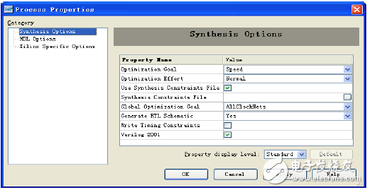
2. Comprehensive parameter settingGenerally, when using XST, all properties take the default value. In fact, XST provides rich and flexible attribute configuration for different logic designs. The following describes the XST properties embedded in ISE9.1. Open the design project in ISE, select “Synthesis –XST†in the process management area and right click, the pop-up interface is shown in Figure 5-4.

Figure 5-4 Comprehensive options
As can be seen from Figure 5-4, the XST configuration page is divided into three categories: Synthesis OpTIons, HDL OpTIons, and Xilinx Specific OpTIons. Global goals and overall strategies, HDL hardware grammar rules, and Xilinx-specific structural attributes.
1) Comprehensive option parametersThe integrated parameter configuration interface is shown in Figure 5-4 and includes eight options, as listed below:
[Optimization Goal]: The goal of optimization. This parameter determines whether the synthesis tool optimizes the design based on area or speed. The area prioritization principle saves the logic resources inside the device, that is, the serial logic structure is used as much as possible, but at the expense of speed. The speed priority principle guarantees the overall working speed of the device, that is, the parallel logic structure is adopted as much as possible, but this will waste a lot of logic resources inside the device, so it is at the expense of logic resources.
[Optimization Effort]: The degree of effort of the optimizer. There are two options for [normal] and [high]. For [normal], the optimizer only performs general optimization processing on the logic design, and the result may not be the best, but the synthesis and optimization process is executed faster. If [high] is selected, the optimizer performs iterative optimization and analysis of the logic design and can generate the optimal synthesis and optimization results, which is usually used for high performance and final design; of course, in synthesis and optimization It takes a long time.
[Use Synthesis Constraints File]: Use a comprehensive constraint file. If this option is selected, the comprehensive constraint file XCF is valid.
[Synthesis Constraints File]: Comprehensive constraint file. This option is used to specify the path to the XST synthetic constraint file XCF.
[Global Optimization Goal]: Global optimization goal. The attributes that can be selected include [AllClockNets], [Inpad To]
Outpad], [Offest In Before], [Offest Out After], [Maximm Delay]. This parameter is valid only for FPGA devices and can be used to select logic between selected registers, input pins to registers, register to output pins, or logic between input pins and output pins. .
[Generate RTL Schematic]: Generates a register transfer level view file. This parameter is used to generate an RTL view of the combined results.
[Write Timing Constraints]: Write timing constraints. This parameter is valid only for the FPGA and is used to set whether the timing constraints used in the HDL source code for control synthesis are passed to the NGC netlist file for layout and routing.
[Verilog 2001]: Choose whether to support the Verilog 2001 version.
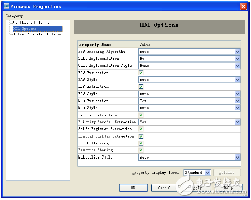
HDL language optionsThe configuration interface of the HDL language option is shown in Figure 5-5, including 16 options, as listed below:

Figure 5-5 Configuration interface options for HDL language options
Wire To Board Connector,Idc Connector,Dip Plug Connector,Box Header Add Housing Connector
Shenzhen Hongyian Electronics Co., Ltd. , https://www.hongyiancon.com