At present, the servo motors in domestic CNC machine tools are generally equipped with incremental encoders, while the accuracy of incremental encoders is not too high and the output is parallel signals. To improve its accuracy, it is necessary to increase the design of the encoder. Difficulty and increase the output of parallel signals, which is not conducive to the long-distance communication between the servo unit and the encoder. The absolute encoder is used, except that its accuracy is several times higher than that of the incremental encoder. High-speed serial communication saves communication lines for long-distance communication. At the other end of the encoder, CPLD and absolute encoder are used for high-speed serial communication. The CPLD then converts the received encoder information into parallel data transmission. The DSP in the servo unit performs arithmetic control. This paper will give the software and hardware design of high-speed serial communication between CPLD and absolute encoder .
hardware design
The hardware is mainly composed of three modules: power supply, CPLD and its peripheral circuits and absolute encoder interface circuit.
Power module
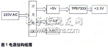
The power module consists of a switching power supply circuit and a DC/DC power supply chip, as shown in Figure 1.

The switching power supply in the figure converts the 220V AC grid voltage into +5V, +15V, -15V. The switching power supply can filter out various interferences in the power grid, and the transformer in the switching power supply will be 220V AC and the output is +5V, + 15V, -15V is isolated, the internal circuit also uses TL431 to adjust the conduction pulse width of the switch tube, so the anti-interference, safety, stability and voltage regulation of the switching power supply are better. The TPS7333 is a DC/DC chip. The +5V DC voltage is converted to a stable DC voltage of +3.3V for use by the CPLD. The TPS7333 has better conversion efficiency, reliability and voltage regulation. It can be used in the voltage range of +3.77V-+10V. Converting +3.3V causes the CPLD to burn out due to the input voltage being too high.
CPLD and its peripheral circuit modules
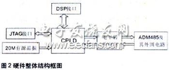
The CPLD and its peripheral circuit modules are mainly composed of CPLD, CPLD programming download interface circuit (JTAG interface), DSP interface circuit, active crystal oscillator, level conversion circuit and ADM485 and its peripheral circuits (interface circuit responsible for communication with the encoder). figure 2).

This design CPLD uses Altera's EPM570T144C5, which belongs to Altera's MAX II. MAX II is lower in cost than MAX I, and consumes less power. The device has more macro cells and the device delay is controlled within 6 ns. With high cost performance, the EPM570T144C5 has 570 macrocells. The number of pins on the chip is 144, of which 116 are available I/O ports, so the resources of this chip are sufficient. The CPLD is mainly responsible for high-speed serial communication with the absolute encoder, and is controlled by the DSP command to forward the encoder data and other information to the DSP in parallel.
The JTAG interface is mainly used to download the executable file to the CPLD, install the development environment of the Altera company - QUARTUS II on the PC, and compile the written VHDL program in this development environment to ensure that the compilation is not error-free and the function is implemented. Connect the download cable to the JTAG interface and download the CPLD board through the programming download tool provided by QUARTUS II.
The DSP interface consists of 8 data lines, 3 address lines and 1 control line. The 8 data lines are responsible for transferring the encoder data and other information. The 3 address lines are responsible for transmitting DSP commands and decoding at the CPLD terminal. The CPLD transmits the encoder data or other information to the DSP through 8 data lines according to the decoded command. The control line mainly completes the synchronous control of the CPLD and the DSP.
The 20M active crystal oscillator mainly provides a reference clock for the CPLD. Under the driving of the clock signal, the CPLD generates a baud rate of 2.5Mb/s to communicate with the encoder, and generates a 10M Hz clock for some logic control signals. Providing a clock frequency of 20M Hz requires a 3.3V DC voltage from the power supply.
The level shifting circuit is mainly responsible for converting 3.3V to 5V or 5V to 3.3V, because the core and I/O ports of the CPLD require a supply voltage of 3.3V, which is required for ADM485 and absolute encoders. Both the supply voltage and the I/O port driver circuit are 5V, so it is necessary to convert 3.3V to 5V or 5V to 3.3V with the level conversion chip LVC4245A.
ADM485 and its peripheral circuits are the hardware connection between CPLD and absolute encoder high-speed communication. The working voltage of ADM485 is 5V, and its maximum communication speed is 5Mb/s. The use of two ADM485 chips for docking communication can improve the anti-interference ability on the communication line, and the longest transmission distance can reach 1.2km. The peripheral circuit is shown in Figure 3. The right half of the dotted line belongs to the peripheral circuit of the absolute encoder. The pull-up and pull-down resistors are 1K ohms, the current limiting resistor is 220 ohms, and the ADM485 SDAT is the data output pin. ADM485 is SRQ is the data input pin, DE of ADM485 is the external control pin, this pin is controlled by CPLD. Since RS-485 communication protocol is half-duplex, ADM485 can only be in the state of sending data or receiving data. When ADM485 is DE high, ADM485 is in data output state (that is, CPLD receives data). When DE of ADM485 is low level, ADM485 is in data input state (that is, CPLD sends data).
Connector 2.5Mm Pitch,S11 Connectors,Welding Bar Connectors,Pressure Weld Bar Connector
YUEQING WEIMAI ELECTRONICS CO.,LTD , https://www.weimaiwafer.com