Electromagnetic compatibility EMC (Electromagnetic compaTIbility)
For equipment or system performance indicators, it is literally translated as "electromagnetic compatibility";
But as a discipline, it should be translated as "electromagnetic compatibility".
The national standard GB/T4365-1995 "Electromagnetic Compatibility Terminology" defines electromagnetic compatibility as "the ability of a device or system to work normally in its electromagnetic environment and does not constitute unbearable electromagnetic disturbance to anything in the environment."
Simply put, it is the ability to resist interference and the degree of external harassment.
Electromagnetic compatibility is a science that studies the coexistence of various electrical equipment (sub-systems, systems; including biological entities in a broad sense) under the conditions of limited space, limited time, and limited spectrum resources.
2. Basic conceptsElectromagneTIc compaTIbility (EMC) Electromagnetic compatibility—The ability of electronic products to work in an electromagnetic environment without reducing function or damage;
ElectromagneTIc interference (EMI) Electromagnetic interference-the process by which the electromagnetic energy of electronic products is transmitted through conduction or radiation; it is composed of three elements: interference source, coupling channel and interfered receiver.
Radio frequency (RF) radio frequency, radio frequency-the frequency range used for communication, about 10kHz to 100GHz. These energy can be generated intentionally, such as wireless telex transmitters, or unintentionally generated by electronic products; RF energy is transmitted through two modes:
Radiated emissions (RE)—The electromagnetic field of this type of RF energy is transmitted through the medium; RF energy generally propagates in free space, however, other types may also occur.
Conducted emissions (CE)—The electromagnetic field of this type of RF energy propagates through the question medium, generally through wires or internally connected cables; Line Conducted interference (LCI) refers to the RF energy on the power line.
Susceptibility tolerance, tolerance-relative measurement of the degree of confusion or damage a product is exposed to in an EMI environment.
Immunity-a relative measurement of the product's ability to withstand EMI;
Electrical overstress (EOS) electronic excessive high voltage-when encountering high voltage surge products suffered damage or just loss of function; EOS includes lightning and electrostatic discharge events.
Electrostatic discharge (ESD) Electrostatic discharge-a high-voltage pulse that may damage or lose functions of the affected products. Although lightning is also a high-voltage pulse, ESD generally refers to less amperage and is thickened by the human body. It is caused by triggering; under normal circumstances, lightning strikes are also regarded as ESD categories, because their protection methods are very similar, but the size is different.
Radiated susceptibility (RS) radiation tolerance-the product's ability to withstand EMI propagated through free space.
Conducted susceptibility (CS)-the product's ability to withstand electromagnetic energy transmitted through external cables, power lines and other I/O cables;
Containment-To prevent RF energy from escaping from an enclosed object (enclosure), usually a metal shield (Faraday cage), or a plastic shell with conductive paint. Based on the mutual principle, we can also view containment as preventing RF energy from entering the enclosure.
Suppression Suppression-designed to reduce or eliminate RF energy at the source, so that it does not rely on second-order methods such as metal enclosures.
3. Types of electromagnetic interference sourcesThere are many types of electromagnetic interference sources, which can be classified in different ways. The interference sources that directly affect the measurement and measurement equipment in the measurement environment can be divided into natural interference sources and man-made interference sources.
Natural interference sources include:
(1) Atmospheric noise interference: such as spark discharge caused by lightning, which belongs to pulse broadband interference, and its coverage ranges from several Hz to more than 100MHz. The distance of propagation is quite long.
(2) Solar noise interference: refers to the radiation noise of sunspots. During the sunspot activity period. The outbreak of sunspots. It can produce strong noise thousands of times higher than the stationary period. Caused communication interruption.
(3) Ning Zhou noise: refers to the noise from the celestial bodies in the universe.
(4) Electrostatic discharge: The electrostatic voltage accumulated on the human body and equipment can be as high as tens of thousands of volts to hundreds of thousands. It is often discharged by corona or spark, which is called static discharge. Electrostatic discharge generates powerful instantaneous currents and electromagnetic pulses, which can cause damage to electrostatic sensitive devices and equipment. Electrostatic discharge belongs to pulse broadband interference, and the frequency spectrum component is continuous from DC to mid-frequency.
Man-made interference sources refer to electromagnetic interference generated by electrical and electronic equipment and other artificial devices. The man-made interference sources mentioned here all refer to unconscious interference. As for the interference that is deliberately released to achieve a certain purpose, such as electronic countermeasures, it is not within the scope of this article.
Any electrical and electronic equipment may cause human interference. Here, just mention some common interference sources that interfere with the measurement environment.
(1) Radio transmission equipment: including mobile communication systems, broadcasting, television, radar, navigation and radio relay communication systems. Such as microwave relay, satellite communication, etc. Due to the large transmitted power, the fundamental signal can produce functional interference; harmonic and spurious emission constitute non-functional unwanted signal interference.
(2) Industrial, scientific, and medical (ISM) equipment: such as induction heating equipment, high-frequency welding machines, X-ray machines, high-frequency physical therapy equipment, etc. In addition to interference from space radiation, the powerful output power also interferes with distant equipment through the industrial frequency power network.
(3) Power equipment: including servo motors, electric drills, relays, elevators, etc., the sudden current changes produced by the on and off of equipment and the accompanying electric sparks become interference sources: non-linear loads in the power system (such as electric arc furnaces, etc.), intermittent power supplies ( UPS) Equivalent power conversion equipment produces a large number of harmonics flooding into the power grid as a source of interference: fluorescent lamps and other lighting equipment also produce glow discharge noise interference.
(4) Automobile and internal combustion engine ignition system: The automobile ignition system produces broadband interference, and the interference intensity is almost unchanged from several hundred kilohertz to several hundred megahertz.
(5) Grid interference: Refers to the interference caused by the strong electromagnetic field and earth leakage current of the 50Hz AC power grid, as well as the micro-arc caused by poor contact such as corona and insulation fracture of high-voltage transmission lines and electric sparks on the surface of contaminated conductors.
(6) High-speed digital electronic equipment: including computers and related equipment.
In terms of the mechanism of the above-mentioned electromagnetic interference, there are discharge noise (lightning, electrostatic discharge, glow discharge, etc.). Contact noise, circuit transition phenomenon, electromagnetic wave reflection phenomenon, etc. The electromagnetic wave reflection in the transmission line is a source of interference that high-frequency measurement and digital equipment must take seriously.
Fourth, the coupling channel of electromagnetic interferenceAn important element in electromagnetic interference is the coupling channel. In many cases, it is difficult to find the real interference source, and it is difficult to improve the interfered receiver. At this time, the most feasible solution is to interfere with the interference in the coupling channel. The coupling is sufficiently attenuated.
Five, coupling channel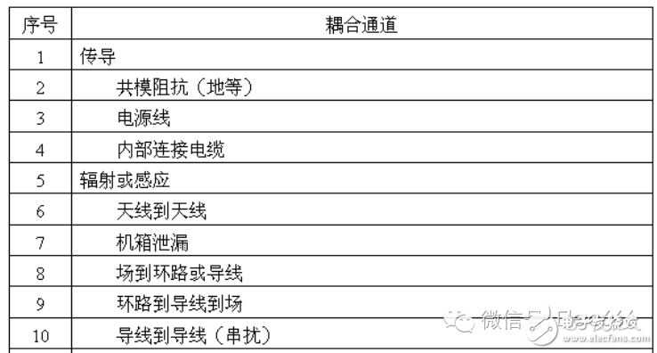
There are two ways of transmission of electromagnetic interference: conduction transmission and radiation transmission. From the perspective of the disturbed sensor, the coupling of interference can be divided into conduction coupling and radiation coupling.
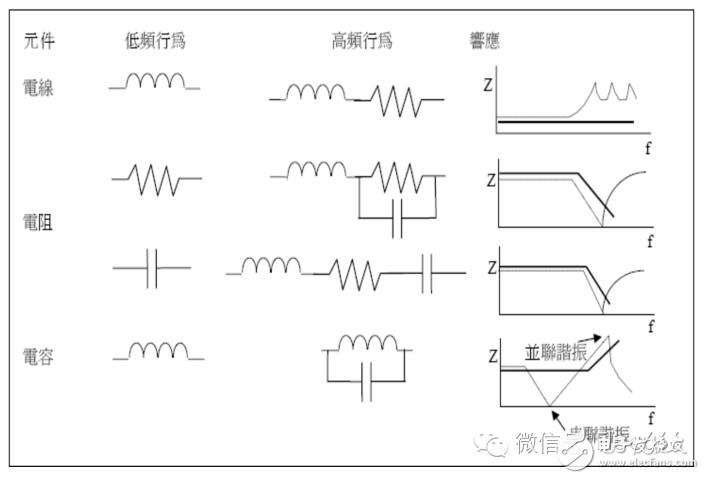
1. Resistive coupling

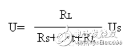
The interference source is directly coupled to the receiver through the resistance Rt of the wire. Suppose Us is the interference voltage and Rs is the internal resistance of the interference source, then the voltage on the receiver is:
2. Capacitive coupling
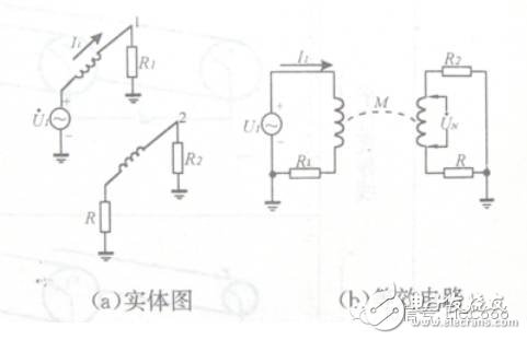
Circuit A and circuit B are capacitively coupled through two wires. Also known as electric field coupling.
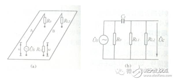
In radio frequency circuits, cables with multiple wires, the interference on one wire can be coupled to all other wires, so high-frequency signal wires must be shielded. Distributed capacitive coupling is most likely to occur between the pins of the high-frequency amplifier transistor, and the lead length of the pins should be shortened as much as possible.
3. Inductive coupling
When a changing current flows in a circuit, a changing magnetic field will be generated in the space around it, and this changing magnetic field will induce a voltage in adjacent loops, thus coupling an interference voltage to the receiving circuit. Inductive coupling is also called magnetic field coupling.
1. Common ground impedance coupling
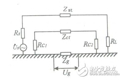
In the figure, Us is the interference source voltage, Rs is the internal resistance of the interference source, RL is the load of the interference source loop, Zst is the impedance of the interference source loop, Rc1 and Rc2 are the internal resistance and load of the interfered loop, and Zct is the interfered loop. The connection impedance. Zg is the common ground impedance.
In the interference source loop, there is generally RS+ZST+RL>>Rg, so the loop current I1 can be obtained as:
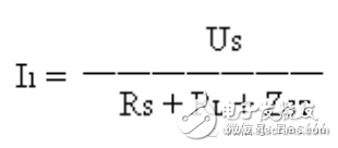
The interference voltage Ug caused by I1 on the common ground impedance is:

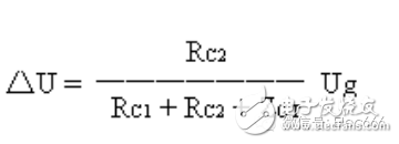
The voltage drop Ug of common ground impedance causes additional interference voltage â–³U on load RC2 in the receiving circuit:
2. Common power coupling
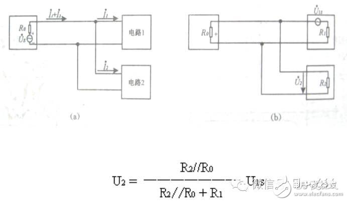
It can be seen that interference signals generated in any load circuit will be coupled to other load circuits through the internal resistance of the power supply. From the above formula, it can be seen that if R0=0, that is, the power supply has no internal resistance, the interference will not be conducted. In fact, the internal resistance of the power supply It cannot be zero.
8. International standards and national standards for electromagnetic compatibilityThere are many international standards related to electromagnetic compatibility, including the US military standard MIL/ANSIC/AIR, the International Special Committee on Radio Interference (CISPR) standard, the US Federal Standard FED/FCC, the German Standard DIN/VDE, the Largest Standard C, and the British Standard BS , ISO, CEN, IEC, etc. The current national standards commonly used in China are GB/T 17626, GB9254 and GB6833, which correspond to the International Electrotechnical Commission standard IEC 61000.
Nine, EMC test items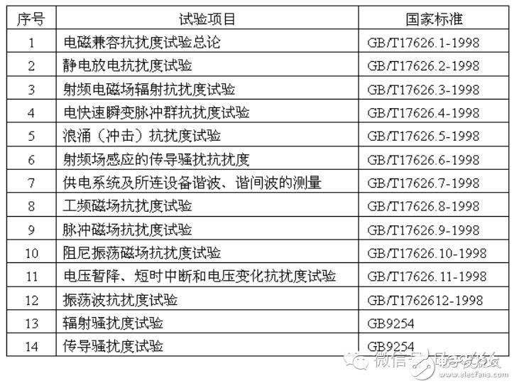
The electrostatic discharge immunity test evaluates the antistatic ability of the equipment, and applies electrostatic interference to the equipment shell and parts that can be touched by human hands to check whether the equipment can work normally. There are corresponding level requirements and test methods.
The electrical fast transient pulse group immunity test assesses the anti-pulse interference ability of the equipment, imposes regular pulse interference on the equipment power supply, and checks whether the equipment can work normally. There are corresponding level requirements and test methods.
The surge (impact) immunity test examines the anti-surge capability of the equipment, applies high-energy pulse interference to the equipment power supply, and examines whether the equipment can work normally. There are corresponding level requirements and test methods. Generally used to assess power supply.
The radiation disturbance test examines the degree of external radiation interference of the equipment. A standard antenna is used in the microwave anechoic chamber to receive the radiation signal when the equipment is working. There are corresponding level requirements and test methods.
Conducted disturbance test investigates the degree of external conducted interference of the equipment. Standard equipment is used in the shielded room to receive the interference signal conducted from the power line when the equipment is working. There are corresponding level requirements and test methods.
10. Electromagnetic compatibility measuresThe electromagnetic compatibility design of the equipment includes the following steps:
1. Component selection and circuit design
2. Application of filtering technology
3. Grounding design
4. Application of shielding technology
5. Circuit layout and equipment layout planning
6. Classification and laying of wires
7. Component selection and circuit design
The source of electromagnetic compatibility should do a good job in the selection of components and circuit design, because components are both the interference source and the interfered receiver, reduce the external electromagnetic interference amplitude of the interference source, and choose the appropriate cost-effective element with strong anti-electromagnetic interference ability. Devices are the most effective way to improve electromagnetic compatibility.
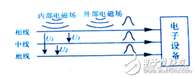
11. Application of filtering technologyThe interference in the power supply is divided into two types: common mode interference and differential mode interference. The interference between the phase line and the ground line of the power line is common mode interference, such as U1 in the figure; the interference between the neutral line and the ground line is also common. Mode interference, such as U2; and the interference existing between the line phase and the neutral line is called differential mode interference, such as U3. Differential mode interference currents are equal in phase and neutral, but opposite in phase. Common mode interference exists in the phase line and the neutral line at the same time, with the same magnitude and the same phase.
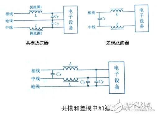
In fact, common mode and differential mode interference often exist in the power line at the same time. Therefore, a practical power supply filter is composed of a common mode filter circuit and a differential mode filter circuit, as shown in the figure:
Grounding originally meant to connect to the real earth to provide a path for lightning discharge. For example, one end of a lightning rod was buried in the earth, and later it became a technical measure to provide leakage protection for electrical equipment and power facilities.
Now the meaning of grounding has been extended. It generally refers to the technical behavior of connecting to a good conductor as a reference potential point (or surface). The "ground" is not necessarily the actual earth, but generally refers to a certain part of the circuit and system. Metal conductive plate wire, it can be used as a common potential reference point for any electrical signal of each circuit in the system. The ideal grounding conductor is a zero resistance entity. Any current flowing through the grounding conductor should not produce a voltage drop. There should be no potential between them, but improper grounding will introduce electromagnetic interference.
Generally, the circuit is divided into four categories according to signal characteristics, and grounded separately to form four independent grounding systems. Each "ground" system may use different grounding methods.
The first category: sensitive signal and small signal "ground" system. Including low-level circuits, weak signal detection circuits, sensor input circuits, pre-amplifier circuits, mixers, etc. Because these circuits have low operating levels and weak signal amplitudes, they are particularly susceptible to failure or degradation due to interference, so their ground Lines should not be mixed in other circuits.
The second category: Grounding systems for insensitive signals and large signal circuits. It includes high-level circuits, final amplifiers, high-power circuits, etc. Because the working current in these circuits is relatively large, and the current in the ground wire system is also relatively large, it must be set separately from the ground wire of the small signal circuit, otherwise the coupling effect of the ground wire will inevitably cause interference to the small signal circuit and make the circuit Can not work normally.
The third category: the system of interference source equipment, which includes motors, relays, contactors, etc. Since sparks or rush currents generated by such components often cause serious interference to electronic circuits, in addition to shielding isolation technology, the ground wire must be set separately from the electronic circuit.
The fourth category: is the metal component ground. It includes casing, bottom plate, door, panel, etc. In order to prevent personal electric shock accidents, lightning accidents, interference from external electromagnetic fields, and static electricity generated by friction, the chassis must be grounded.
13. Classification principle of grounding system
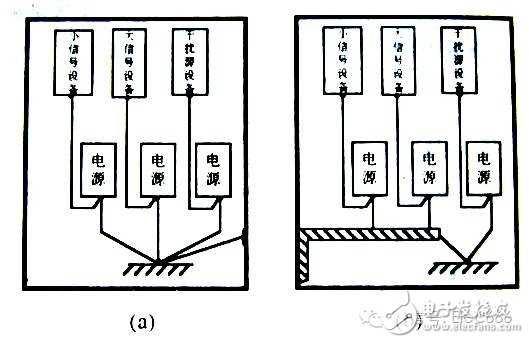
1. Single point grounding system
In this case, the ground potential of each device (or each branch) is only related to the respective ground current I and ground wire, and is not affected by other circuits. It is very effective to prevent interference between circuits and ground loop interference. . Especially when the circuit frequency is low and the connecting wire is relatively short, this grounding method is often used. Its disadvantage is that it is not suitable for high frequency circuits.
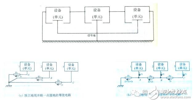
2. Multi-point grounding system
Multi-point grounding means that each unit circuit in the equipment is directly connected to the ground line, and there are multiple grounding points, as shown in the figure. For high-frequency circuits, in order to reduce ground wire impedance, multi-point grounding is generally used. The ground wires used in the figure are connected to the nearest low-impedance ground wire. The ground wire system is generally a flat thick metal conductor connected to the case or the case itself, and its inductance is very small.
The advantage of the multi-point grounding system is that the circuit structure is simpler than single-point grounding, and because the grounding wire is short, the high-frequency standing wave phenomenon that may appear on the grounding wire is significantly reduced. However, after multiple points are grounded, many ground loops will be added inside the equipment, which will cause interference to lower level circuits and bring adverse effects.

3. Mixed grounding system
In some electrical equipment, there are both high frequency part and low frequency part. At this time, it should be treated separately. The low-frequency circuit should be grounded at a single point, and the high-frequency circuit should be grounded at multiple points. This grounding system is called a mixed grounding system, as shown in the figure.
The actual situation of electrical equipment is more complicated, it is difficult to solve the problem through a simple grounding method, so the application of mixed grounding system is more common.
 14. Application of shielding technology
1. Electrostatic shielding
Suppose a positively charged conductor A, if there is a conductor B nearby, the conductor B will be negatively charged due to electrostatic induction, as shown in the figure.
If the conductor A is surrounded by a metal shield, the same amount of negative charge as that of the conductor A is induced on the inside of the shield, and the same amount of positive charge appears on the outside, and the lines of force will continue to reach B, making the induced electric field more Is complicated. If the metal shield is grounded so that the electric field outside the shield disappears, the conductor B will not be subject to inductive interference. This is the principle of electrostatic shielding.
Electrostatic shielding should have two basic points: perfect shielding and good grounding.

2. Magnetic shielding
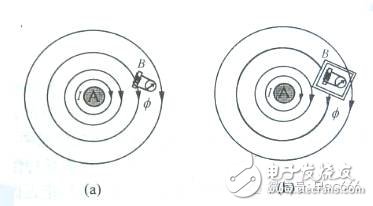
Magnetic shielding is a measure used to isolate magnetic field coupling. There is a magnetic field around any current-carrying wire or coil. As shown in figure (a), there is a current I in wire A, and there is a magnetic field around the wire. A series of concentric magnetic lines of force are used It means that in order to prevent the magnetic field from interfering with the adjacent element B, a material with high magnetic permeability can be used to surround B, so that the magnetic lines of force are concentrated in the shield, so that the sensitive element B is protected, as shown in Figure (b).
Since the magnetic permeability of the magnetic shielding material is tens of times or even thousands of times greater than that of air, most of the magnetic lines of force are concentrated in the shielding layer and pass through, so that element B is protected from interference.
Magnetic field shielding is different from electric field shielding. The shielding body will not affect the shielding effect if it is not grounded. However, since the magnetic shielding material also has a certain shielding effect on the electric field, it is usually grounded.
3. Electromagnetic shielding
Electromagnetic shielding is an effective method to prevent alternating electromagnetic field induction and radiation interference.
There are three types of electromagnetic fields: alternating electric field, alternating magnetic field and alternating electromagnetic field. The shielding principles and methods for the three fields are different.
1). Alternating electric field shielding
The principle of alternating electric field shielding is to use a well-grounded metal shield to limit the alternating electric field generated by the field source in a certain space, thereby blocking the electric field propagation path from the interference source to the sensitive circuit.
2). Alternating magnetic field shield
The shielding of the alternating magnetic field can be divided into high-frequency magnetic shielding and low-frequency magnetic shielding. The principle of low-frequency magnetic shielding is the same as that of static magnetic shielding. Typical applications are relay packaging, power transformer packaging, and filter packaging. High-frequency magnetic shielding is to use the diamagnetic field of the eddy current generated by the shielding body to cancel the interfering magnetic field, and use this principle to achieve shielding. Therefore, high-frequency magnetic shielding uses high-conductivity materials, such as copper, aluminum, etc., and a typical application is mid-peripheral transformers in radios.
3). Alternating electromagnetic shielding
Electromagnetic shielding is a technical measure to prevent high-frequency radiation electromagnetic waves from spreading in space with a shielding body. The shielding body plays a role in cutting off or weakening the transmission of electromagnetic waves.
When the alternating electromagnetic field passes through the metal material shield, the metal material will generate an induced electric potential to form an eddy current. The magnetic field generated by the eddy current can offset a part of the original magnetic field, thereby acting as a shield. The greater the eddy current, the stronger the shielding effect, so the greater the conductivity of the shielding material, the better the shielding performance. The higher the electromagnetic field frequency, the stronger the shielding effect.
15. Implementation of electromagnetic compatibilityPower supply: Since a lot of electromagnetic interference is coupled to electronic equipment through the power supply, special electromagnetic compatibility design is done on the system power supply. Increase effective voltage transformation, voltage stabilization, and filter circuits, and use high-efficiency switching power supply chips and low-dropout linear power supply chips with good voltage stabilization and filtering effects to provide stable and reliable power for the system.
2. Use decoupling capacitor: Add a decoupling capacitor between the power supply and ground of each integrated circuit. The decoupling capacitor has two functions: on the one hand, it is the energy storage capacitor of the integrated circuit, which provides and absorbs the charging and discharging energy at the moment of opening and closing of the integrated circuit; on the other hand, it bypasses the high frequency noise of the device.
3. Ground wire separation: A 4-layer circuit board design is adopted to reduce the parasitic inductance of the power supply and ground, and effectively enhance the EMC performance of the system. Separate power layer and ground layer can effectively prevent the coupling between the devices through the ground wire and the power supply. In addition, the method of segmentation and isolation is adopted for ground wires with different properties, so that the currents of the ground wires of different properties can take different paths, which can prevent Signal crosstalk.
Communication interface: The system’s 485, 232, USB and other communication interfaces are connected with external cables and have direct contact with external equipment, so they are also vulnerable to various electromagnetic interference. In order to enhance the anti-interference ability of these communication interfaces, string the communication signal lines Connect magnetic beads and parallel varistors, and filter capacitors;
In addition, in order to enhance immunity and reduce harassment, the following principles should be followed when arranging PCB boards:
1. The quartz crystal oscillator should be as close as possible to the device using the clock, the clock line should be as short as possible, the shell should be grounded, and the clock area should be circled with the ground line.
Do not route wires under the quartz crystal and under noise-sensitive devices.
2. The I/O drive circuit should be as close as possible to the edge of the printed board, and let it leave the printed board as soon as possible. The signal entering the printed board should be filtered, and the signal from the high-noise area should also be filtered. At the same time, a series of terminal resistors should be used to reduce signal reflection.
3. The useless end of MCU should be connected to high, or grounded, or defined as the output end, and the end of the integrated circuit that should be connected to the power supply ground should be connected, and do not float. Do not leave unused gate circuits floating.
4. The printed board should try to use 45-fold lines instead of 90-fold lines to reduce the external emission and coupling of high-frequency signals.
5. Correctly choose single-point grounding and multi-point grounding. In the low-frequency circuit, the working frequency of the signal is less than 1MHz, and the inductance between its wiring and the device has less influence, and the circulating current formed by the grounding circuit has a greater influence on interference, so one point grounding should be adopted. When the signal operating frequency is greater than 10MHz, the ground wire impedance becomes very large. At this time, the ground wire impedance should be reduced as much as possible, and the nearest multiple points should be used for grounding. When the operating frequency is 1~10MHz, if one-point grounding is used, the length of the ground wire should not exceed 1/20 of the wavelength, otherwise the multi-point grounding method should be used.
6. Separate the digital circuit from the analog circuit. There are both high-speed logic circuits and linear circuits on the circuit board. They should be separated as much as possible, and the ground wires of the two should not be mixed, and they should be connected to the ground wires of the power supply. Try to increase the grounding area of ​​the linear circuit.
7. Make the ground wire as thick as possible. If the grounding wire is very thin, the grounding potential will change with the change of the current, causing the timing signal level of the electronic equipment to be unstable and the anti-noise performance to deteriorate. Therefore, the ground wire should be as thick as possible so that it can pass three times the allowable current of the printed circuit board. If possible, the width of the ground wire should be greater than 3mm.
8. Form the ground wire into a closed loop. When designing the ground wire system of the printed circuit board composed of only digital circuits, making the ground wire into a closed loop can significantly improve the anti-noise ability. The reason is that there are many integrated circuit components on the printed circuit board, especially when there are components that consume more power, due to the limitation of the thickness of the ground wire, a large potential difference will be generated on the ground junction, which will cause the anti-noise ability to decrease , If the grounding structure is formed into a loop, the potential difference will be reduced and the anti-noise ability of electronic equipment will be improved.
9. Choose a reasonable wire width. Since the impact of the transient current on the printed lines is mainly caused by the inductance of the printed wires, the inductance of the printed wires should be minimized. The inductance of the printed wire is proportional to its length and inversely proportional to its width, so short and precise wires are beneficial to suppress interference. The signal lines of clock leads, row drivers or bus drivers often carry large transient currents, and the printed wires should be as short as possible. For discrete component circuits, when the printed wire width is about 1.5mm, it can fully meet the requirements; for integrated circuits, the printed wire width can be selected between 0.2mm and 1.0mm.
10. Adopt the correct wiring strategy. The use of equal routing can reduce the wire inductance, but the mutual inductance and distributed capacitance between the wires increase. If the layout allows, it is best to use a grid-shaped wiring structure. The specific method is to wire one side of the printed board horizontally and the other side to wire vertically. Then connect with metallized holes at the cross holes. In order to suppress the crosstalk between the conductors of the printed circuit board, long-distance equal routing should be avoided when designing the wiring.
Android is an open source mobile operating system based on Linux platform released by Google at the end of 2007, and then improved for use in netbooks and MIDs. The platform consists of operating system, user interface and application software, and is claimed to be the first truly open and complete mobile software for mobile terminals.
To put it simply, the Android system is actually a very open system. It can not only realize the functions of the most commonly used notebook computers, but also realize various directional operations like mobile phones. Moreover, it is specially designed for mobile phones. The operating system developed for equipment has advantages in system resource consumption and human-computer interaction design. It is an operating system that combines traditional and advanced advantages.
New Android Tablet,Android Tablet,New Android Tablet
Jingjiang Gisen Technology Co.,Ltd , https://www.jsgisentec.com