With advances in overmolding plastic packaging technology, developers of high-power RF transistors can reliably package devices in a way that rivals ceramics.
Packaging is critical to achieving optimal performance of RF power transistors. Since RF power transistors are one of the most expensive components in power amplifiers (PAs), and PA is the most expensive component in cellular base stations, how to reduce the cost of transistors without sacrificing performance is highly valued. Supermode compression molding technology provides a solution that has been accepted by other power integrated circuit (IC) applications, but has only recently been fully improved to meet the needs of RF power transistor developers. This technology provides the technical performance we need at an order of magnitude lower than existing packaging methods.
Innovative technologies that increase the price/performance of RF power semiconductors are likely to affect the future direction of 2.5G and 3G wireless networks. High power RF transistors have traditionally been fabricated in leaded ceramic packages. In the base station, the power transistors are mounted on a printed circuit board (PCB), just as the circuit board is plugged into the cellular base station as the line card of the telecom central office equipment. A typical cellular/radio base station has approximately 8 to 10 PAs. Power transistors are the most expensive components in PA, and their cost accounts for a very large proportion of the total cost of all base stations. In addition, approximately 30% of base station problems are related to PA, so PA reliability is critical to the successful operation of wireless networks.
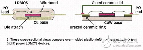
In view of the performance and reliability requirements of RF power transistors, they are typically mounted in a package that combines a thermally conductive metal base and a ceramic ring to separate the input and output leads. The base is made of copper-tungsten alloy and covered with metal for attachment to the ceramic ring through a high temperature brazing process. Due to the ceramic ring, the first generation solution is called ceramic package. In addition, the package base is gold plated to attach the die to it through a second high temperature process. The package incorporates a ceramic cover that is attached to the ceramic ring and the input and output leads as the only environmental measure.
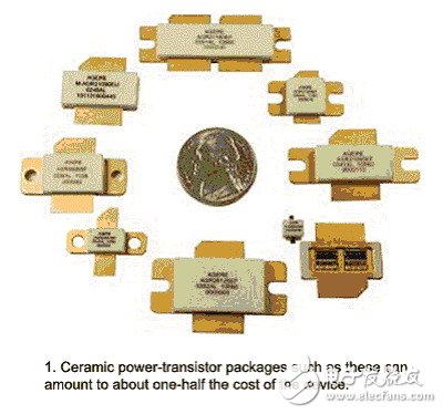
With ceramics, the cost of packaging is almost half of the total cost of a finished power transistor (see Figure 1). Of course, for RF transistors, the package not only protects the die, but also provides a way to receive electricity and dissipate excess heat. In fact, packaging is not only a key factor in achieving high performance, but also a cost reduction requirement for many microelectronics and computer systems. In fact, the RF package must provide:
1. Connection of the power and signal lines of the installed chip
2. Attach the base of the active die and all related components
3. Ways to dissip excess heat
4. Structure that protects and maintains connection and chip integrity while providing a platform for operation and external identification for easy identification.
Obviously, the way to reduce costs is to eliminate expensive ceramic rings and cumbersome and expensive copper welding processes. Fortunately, innovations in polymer materials (plastics) make this a reality. Two synthetic polymers can be used: thermoplastics and thermosets. The thermoplastic is processed only by heating and pressurization without a chemical reaction therebetween. After cooling, the thermoplastic either crystallizes or turns into a glassy state. The thermosetting polymer (epoxy plastic, phenolic plastic, formica plastic) undergoes a chemical reaction upon heating, resulting in an increase in molecular weight. This chemical reaction results in complete conversion of all reactive groups, resulting in a polymer with high hardness, high thermal distortion temperature, and good chemical and physical resistance.
When a semiconductor package is packaged with a polymer, the chip is connected to the package lead frame by wire bonding and then encapsulated in a polymeric insulator, which acts as an electrical insulator and a protective layer to prevent environmental impact. Figure 2 provides a comparison of ceramic and overmolded plastic packages.
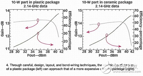
The overmolded package does change the RF performance. In ceramic packages, both the chip and the bond wire are in the air holes. In plastic packages, the polymeric material encases and contacts the equipment and bonding wires. Since the dielectric constant of the polymer is higher than that of air, the parasitic effect in the plastic package is higher, so the output power and gain are slightly lower than those in the same ceramic package. However, by using appropriate device design, layout, and wire bonding techniques, the effects of parasitic effects on plastic packages can be reduced to 0.5 dB (see Figure 3).
In March 2003, Allertown (PA) introduced 21 new breakthrough transistors for the wireless base station PA market. Based on traditional ceramic packaging, these products enable users to build wireless base stations that produce less heat, are smaller, and are less expensive. The thermal performance of these semiconductor products has reached a new level, reducing the number of cooling fans in the base station by half, enabling service providers to reduce capital and operating costs while reducing fan noise pollution. Agere Systems is now moving to next-generation RF transistor devices that are packaged in high-capacity overmolded packages (see Figure 4).
Early implementation of plastic packaging solutions reduced costs, however, the use of internal assembly lines hindered further cost reductions. The use of high-capacity packaging devices is more attractive, sharing investment costs, knowledge and innovative technology across multiple product lines. This is very similar to the experience of significantly reducing costs with integrated circuit design companies that use world-class external processing.
Agere's latest RF power product line is packaged in Amkor Technologies' West Chester, PA's Power Small Outline Package (PSOP). To date, the output of this package has reached nearly 1 billion, with high throughput, low cost and high reliability required by the RF electronics market.
This small, thin product can operate reliably in harsh environments. Manufacturers pay special attention to materials and assembly processes to solve customer problems, including flatness, coplanarity, line sweeping, delamination, solderability and cost. Supermode compression molding technology for RF power transistors also has other important technical and commercial advantages: This package enables RF power transistors to be fabricated through mainstream manufacturing processes that are generally accepted by the electronics and communications industries.
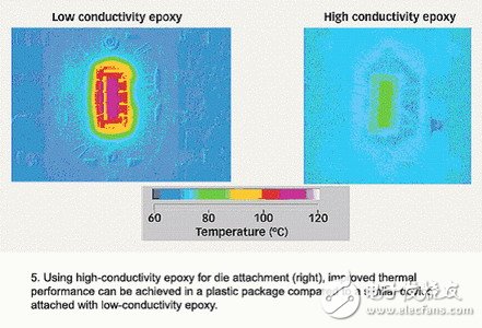
Amkor Technologies' PSOP packaged transistor performance is comparable to that of the same equipment installed in more expensive ceramic packages, providing superior test performance in the 2.1GHz band and significantly reducing costs. These reliable overmolded plastic packages meet current environmental and 2006 environmental standards and are compatible with wireless board technology. In addition, the company demonstrated a new generation of highly conductive epoxy materials that can be used for core tube bonding operations, replacing the wires used in earlier solutions. Agere's overmolded integrated circuits have undergone extensive testing to ensure that low-cost overmolded parts can replace traditional ceramic parts. The overmolded LDMOS components introduced in the second quarter of 2004 will meet the thermal, electromagnetic and physical conditions described in Table 1.
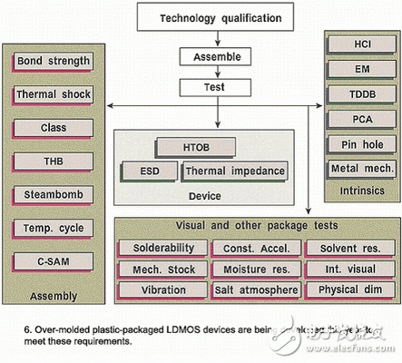
Over time, overmolded RF power transistors will significantly reduce the cost of wireless base station equipment designers and network operators. At the same time, it can reduce power and save space, enabling operators to deploy base stations in new ways. Innovations in packaging technology will certainly drive innovation in other packages. For example, Agere Systems is developing a new venting solution for high output power device devices. In addition, these packaging concepts can be extended to integrated modules to reduce costs even more without compromising performance.
Marine Hatch Cover Pneumatic Winch
Hatch Cover Winches,Portable Pneumatic Winch,Industrial Pneumatic Winch,Marine Hatch Cover Pneumatic Winch
RUDONG HONGXIN MACHINERY CO.,LTD , https://www.rdhxmfr.com