The upgrade from 3G to LTE-Advance presents many challenges for equipment and device vendors for next-generation mobile communications infrastructure. Next-generation wireless devices require a wider signal bandwidth and more complex modulation schemes to achieve higher data rates in a variety of operating bands deployed worldwide. Therefore, performance such as noise, signal linearity, power consumption, and form factor are critical, and these performance requirements are more demanding. In addition, component suppliers are also being asked to reduce the cost and size of components to support higher density applications.
The challenges faced by RF IC designers will also become increasingly difficult as integration solutions must have or exceed the performance achieved by discrete components. When implementing discrete component implementations, system designers can use different technologies (such as GaAs, Si Bipolar, or CMOS) for optimal design. But for RF IC designers who want to offer greater integration through a single process technology, the biggest challenge in choosing the best process technology is flexibility.
Within the transmitter of the base station, the analog I/Q modulator is the key RF IC device that determines the noise floor and linearity of the transmit signal path, and does not sacrifice performance for reducing size, power, or cost.
Fortunately, SiGe BiCMOS process technology enables higher levels of integration without sacrificing performance. These processes typically provide SiGe NPN transistors in a variety of speed categories, and in some cases can provide twice as many (and more often twice) complementary high performance PNP transistors in CMOS transistor feature sizes. On this basis, MIM capacitors, thin film resistors and more important multilayer copper and aluminum metal films can be added. These features enable designers to implement multiple high-performance functional blocks on a single chip, dramatically reducing power consumption, shrinking size, and maintaining high performance.

An important aspect of transmitter board level design is the synthesis and distribution of local oscillator clocks for each of the upconversion and downconversion circuits. The base station local oscillator clock must be allocated for phase consistency to all remote locations on the PCB and must have low in-band noise, wideband noise, and total spurious noise. The performance of the mixer is the same as the performance of the local oscillator that drives it, so a high quality local oscillator is the key to improving the overall performance of the transmitter. In addition, small phase noise or spurious components on the local oscillator signal may introduce enough energy into the analog signal path, causing the transmitter to fail to meet some of the major cellular communication standards (MC-GSM, WCDMA, LTE, WiMAX). ) Specified spurious interference indicators. These standards require a local oscillator frequency range of approximately 500 MHz to approximately 4 GHz, which means that the layout design used for local oscillator clock distribution must be very careful. The length of the trace from the generation of the local oscillator to the final termination should be as short as possible, but this requirement is difficult to satisfy if the local oscillator synthesizer must be fed to multiple different devices. One solution is to feed a common low frequency reference clock to a separate PLL synthesizer near each local oscillator, but this takes up a large PCB area.

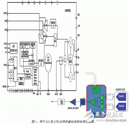
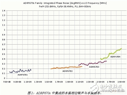
The ADRF670x family of integrated modulators solves many of these problems by integrating advanced fractional-N PLLs and VCOs. The use of silicon germanium technology allows the built-in VCO's quadrature modulators and mixers to achieve industry-leading dynamic range and competitive performance with significantly smaller footprint than external VCO/PLL solutions. The VCO is implemented in the upper thick metal layer, and a high Q on-chip inductor can be used as part of the LC circuit. The VCO capacitor is composed of MOS switch type MIM capacitors, thus allowing the VCO to switch frequencies over a wide frequency range with low phase noise. The frequency band is automatically adjusted each time the PLL frequency is programmed, thus providing an independent and reliable solution. After initialization is complete, the band size is chosen to ensure that the device will operate over the full temperature range. The thick metal layer is also used to integrate an output balun (Balun) with excellent reflection loss. The ADRF670x family consists of four members whose frequency parameters overlap each other, covering the frequency range and frequency band from 400MHz to 3GHz, each of which is defined by the output Balun bandwidth on the 1dB and 3dB passbands.
The ADRF670x and ADRF660x family of fractional-N PLL designs are ideal for low phase noise 3G and 4G applications. These new cellular standards have dense signal constellations that require increasingly low local oscillator phase noise to achieve adequate performance. Traditional PLL synthesizer designs use an "integer N" architecture with an output frequency that is an integer multiple of the phase detector frequency. To provide smaller frequency steps, the integer multiplication factor must be very large. A large amount of local oscillator phase noise originates from the reference path and is amplified by the PLL frequency multiplication factor, which causes high in-band noise at the PLL output. The fractional-N PLL allows the output frequency to have a small step while maintaining a low total multiplier, thus reducing the phase noise amplification compared to an integer-N PLL.
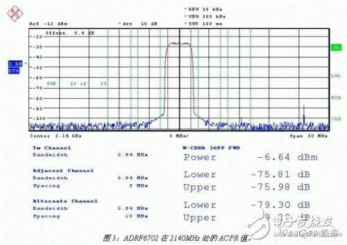
The adjacent channel power ratio (ACPR) is an indicator for judging how much of the transmitted signal leaks into the adjacent frequency band. The 3G standard, such as WCDMA, has strict limits on out-of-band transmit power. The ACPR indicator for the ADRF6702 is shown in Figure 3. The modulator provides highly linear output power and low noise, so there is an ACPR value better than -76dB at the -6dBm output point, which helps reduce the gain stage behind the modulator and the dynamic range in front of the end amplifier stage circuit to reach maximum.

The ADRF670x family of devices integrates three LDO circuits to operate from a single 5V supply, further simplifying user applications, reducing cost and board space. LDO is used to provide stable power to the VCO, charge pump, and PLL delta-sigma modulators. The +5V supply can be used directly in the IQ modulator to maximize output power.
In high-density applications, the ADL670x can use the PLL to perform the internal synthesis of the local oscillator, while other devices can disable their PLL and use a common local oscillator from a certain master device.
The ADRF670x family is designed to simplify the user interface and facilitate connection to ADI's newest transmit digital-to-analog converter, the AD9122 and GaAs amplifiers such as the ADL5320. (The ADL5320 is a 0.25 watt high linearity amplifier capable of driving power above 0 dBm into the final stage power amplifier circuit.) These three compact ICs form a complete active IC device combination that is the next generation of multiple carrier frequencies. Ideal for cellular wireless platforms.
Solar Inverter,Frequency Inverter For Irrigation,Solar Inverter For Pumping System,3 Phase Solar Pump Inverter
Zhejiang Kaimin Electric Co., Ltd. , https://www.ckmineinverter.com