Even for the best analog designers, the design of high voltage amplifier circuits is challenging. Most commercially available amplifiers are limited to use a power supply of ±15V or lower. As semiconductor manufacturing processes use fine line geometries, many new amplifiers are limited to lower voltages, such as 5V or even 3.6V. However, the demand for higher voltage circuits still exists. While discrete circuits can be used to extend the input or output operating voltage range of lower voltage op amps, such practices can be tricky for design reasons due to matching issues, board space limitations, and thermal requirements. The introduction of new high-precision monolithic op amps, including the LTC6090, LTC2057, and LT6016, simplifies the design of high-voltage analog signal links.
The new LTC6090 op amps combine their proprietary circuitry with a layout approach to extend their supply voltage to ±70V without sacrificing the features that high-precision op amps are expected to have. The device uses a MOS input stage design with an input bias current of typically 3pA (at 25°C). The input offset voltage is less than 1.6mV and the noise is 11nV/√Hz (at 10kHz). The input common-mode range extends to within 3V of any power rail (134V across the 140V supply). Its rail-to-rail output stage allows the LTC6090 to drive signals close to the 140VP-P (Figure 1). The LTC6090 is available in a space saving 8-lead SOIC package and a 16-lead TSSOP package. Both packages feature a bare pad for reduced thermal resistance, which facilitates an excellent thermal design. A simple interface to the low voltage control line and built-in thermal safety features simplify high voltage analog design tasks.
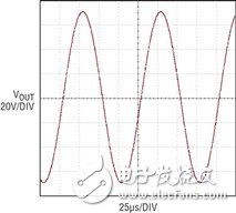
Figure 1: LTC6090 output voltage 140VP-P 10kHz sine wave
High voltage circuit for high dynamic rangeThe example given in Figure 2 shows how to use a high voltage amplifier to improve the dynamic range. Transimpedance amplifier circuits require careful design to achieve low enough noise and high bandwidth. The noise of the circuit depends on the noise generated by the feedback resistor and amplifier. The gain is proportional to the feedback resistor value, which is proportional to the square root of the resistor value. Therefore, the signal-to-noise ratio of the circuit is improved as the resistance increases, and the improvement coefficient is √R. Using a 125V positive supply rail will allow the circuit to operate with a 1MΩ (MV/A) high transimpedance gain value. The output of the amplifier is then attenuated so that the VOUT signal is between 0V and 12V, and the noise is only 21μVRMS (1.75 ppm) in the 1kHz to 40kHz band.
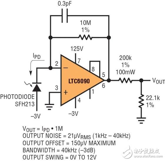
Figure 2: Extended Dynamic Range 1M Transimpedance Photodiode Amplifier
Bias and leakage currentIn photodiodes and other high-impedance transducer applications, the amplifier input bias current must be considered. The low input bias current of the LTC6090 makes it an excellent choice for high impedance applications. As shown in Figure 3, there is a logarithmic relationship between the input bias current and the temperature. The input bias current doubles every 10 °C increase in temperature, but remains low at 125 °C.
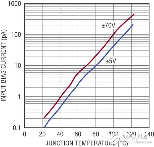
Figure 3: LTC6090 input bias current vs. junction temperature
Since the input can accept high voltages, special care should be taken to avoid leakage currents that can cause measurement errors. In protection-critical applications, it may be beneficial to use a special low-leakage circuit board material as it acts as a guard ring. The LTC6090's TSSOP package includes eight protection pins that can be used to form a guard ring around critical input nodes, as shown in Figure 4. Note that the solder mask should be pulled back through the guard ring to expose the PCB metal. It is important that the PCB be clean and dry. It is recommended to clean the board with solvent and rinse any residue with tap water and then bake the board to remove any moisture. Alternatively, washing the board thoroughly with soap and tap water (without solvent) can also produce good results.
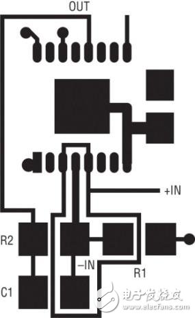
Figure 4: PCB Guard Ring Layout Example
High voltage DAC bufferAnother use for high voltage amplifiers is to buffer lower voltage digital-to-analog converters (DACs). In test equipment, it may be necessary to generate any high voltage to meet the needs of a variety of applications, and in some control applications, large voltage signals are suitable for driving lasers, piezoelectric components, and other transducers or directing beams. As shown in Figure 5, a high voltage amplifier such as the LTC6090 can be used. In this example, a 140VP-P voltage is generated from a 2.5V DAC output.
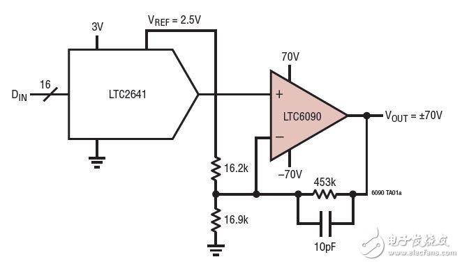
Figure 5: High Voltage DAC Buffer
Hot considerationThe LTC6090 consumes 378mW at a total supply voltage of 140V and a typical quiescent current of 2.7mA. Adding a load will consume more than 1W, so good thermal design becomes a priority. Both the SOIC and TSSOP versions have an exposed pad on the bottom of the package that is internally connected to the negative supply rail V–. The thermal resistance of the package is proportional to the amount of metal soldered to the bare pad, so it is best to connect the bare pad to the largest possible PCB metal plane, as far as practical conditions permit. In the case of a good thermal layout, the thermal resistance SOJA of the SO package is 33 °C / W. When 1W is generated, the junction temperature of the chip will rise to 33°C above ambient temperature.
An important output disable (OD) feature turns off the output stage when the junction temperature becomes too high to prevent the LTC6090 from exceeding the junction temperature of 150°C. This is done by connecting the overheat pin (TFLAG) to the OD pin. When the die junction temperature reaches 145°C, the open-drain TFLAG pin will be pulled low. A 5°C internal hysteresis will cause the TFLAG pin to reset when the junction temperature reaches 140°C. Pulling the active-low OD pin low (relative to the COM pin) turns off the output stage, which in turn reduces the quiescent current of the device to 670μA. The COM pin is common to the OD and TFLAG pins and provides low voltage control of the LTC6090. When the TFLAG and OD pins are tied together, the LTC6090 will be disabled when the die junction temperature reaches 145°C. Note that these pins can be either floating or connected together.
An additional thermal safety feature turns off the output stage when the junction temperature of the die reaches approximately 175 °C. The 7°C internal hysteresis turns the output stage on when the die junction temperature drops back to approximately 168°C. This feature is designed to protect the device from catastrophic thermal faults. Operating the LTC6090 at an absolute maximum junction temperature above 150 °C will reduce its reliability and should be prevented.
in conclusionAmplifiers such as the LTC6090 simplifies high-voltage precision design by providing high-performance specifications for high-performance precision amplifiers while operating from a ±70V supply. The protection pins enable an excellent low-leakage PCB design, while the TFLAG, OD, and COM pins simplify the superior thermal design. The LTC6090, combined with the recently introduced LTC2057 and LT6016, enables a wide range of high voltage circuit designs over ±15V. The LTC2057 features 60V operation, a zero-drift input stage, and low noise operation for optimum accuracy and stable DC performance. The LT6015 / LT6016 / LT6017 are single/dual/quad op amps with an Over-the-Top® input that allows the input common-mode voltage to operate up to 76V above the negative supply rail without the supply voltage influences.
LED TV
GUANGZHOU SOWANGNY ELECTRONIC CO.,LTD , https://www.jerry-power.com