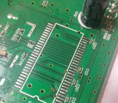
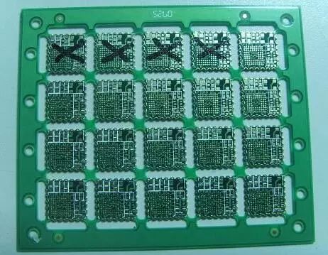
My work is mainly to lead the new product trial production. In the actual work, it often happens that the RD personnel's design "negligence" leads to trial production failure. This negligence should be quoted because it is not caused by genuine carelessness, but by the unfamiliarity of the production process. In order to avoid the same mistakes made by friends who are doing RD, or to complete the trial production better, I will summarize some common problems and hope to help everyone. 1, the choice of IC package. Nowadays, electronic products are developing to lead-free environmental protection. Europe will achieve full lead-free on July 1, 2006. Now it is in the transition period from lead to lead-free. Therefore, components supplied by component manufacturers also have lead-free and lead-free specifications, and some manufacturers have even stopped production of leaded components. The problem lies in the choice of lead and lead-free components. When a product is designed, RD personnel need to confirm the specific components. Please make a lead-free process before confirming the product. The choice of lead technology. If there is no specific determination, the problem is not paid attention to when selecting materials. The presence of lead components and lead-free components in the raw materials can cause difficulties in the SMT process. The peak temperature of the lead-free component is 255 degrees, and the peak temperature of the lead component is not more than 235 degrees. If two materials are mixed, the leaded component will be damaged by high temperature. 2, lead-free components, especially BGA package components, the attached solder ball does not reach the melting point, easily lead to virtual welding or fatigue resistance. Therefore, when determining the components, you must first confirm whether the components are lead-free or lead-free. If the components are lead-free, then the PCB board should be selected accordingly. One aspect is compatible with the lead-free process to make lead-free tin. The solderability of the paste is strengthened. On the other hand, the PCB board used in the lead process cannot withstand excessively high temperatures, which may cause undesirable phenomena such as board warping. 3. The component pad does not match the pad size on the PCB. For various reasons, if the sample supplied by the component supplier is different from the actual one (the batch may be different, the sample may be old), or the component library loaded during the layout is modified by others, etc., and finally the component pad appears. The pad size on the PCB does not match. So you need to check it again before each final production.

4. The component error is too large and the performance is not up to standard. These problems mainly occur in small devices such as capacitors, resistors and inductors. I have encountered a product with a 20% non-performing rate. At the beginning, it was judged that the IC was defective, but the IC that was judged to be bad was replaced with other products that also required this IC. The result was normal, and the reason was found to be because the error standard of a capacitor was large. Achieving the small error requirements of the design, resulting in the test value at the critical point, the final production test is outdated, and a lot of time and manpower is wasted. 5, layout design does not consider SMT machine patch accuracy. This problem is manifested in the small spacing between components, but the SMT placement machine has a minimum precision, if it is less than this minimum precision, it will lead to components flying. 6. The position of the stamp hole is not considered. Usually, the PCB board will make 3 to 4 separate PCB boards into a single board to improve the working efficiency of the SMT, so that the board needs to be cut after the SMT processing is completed. However, after the layout personnel finished designing and delivering the PCB board manufacturer, they did not consider the connection position between the board and the board. It is often the connection position on the component side, and the component design is close to the PCB board. The edge of the edge, which will cause the component to be damaged when the cutting board is broken. Therefore, the position of the stamp hole must also be considered when designing the layout.

7. When the layout is not applied to the BGA package components, it is not convenient for SMT visual inspection.
ASUS ROG Strix NVIDIA GeForce RTX 2060 EVO OC Edition Axial-tech Fan Design, Auto-Extreme 6GB GDDR6 HDMI DisplayPort 1.4 Gaming Graphics Card
1.OC Edition: Boost Clock 1860 MHz (OC Mode)/ 1830 MHz (Gaming Mode)
2.NVIDIA TURING: ROG GeForce RTX graphics cards are powered by the Turing GPU architecture and the all-new RTX platform.
3.DirectX 12: Power new visual effects and rendering techniques for more lifelike gaming.
4.NVIDIA Shadowplay Record and share high-quality gameplay videos, screenshots, and livestreams with your friends.
5.Axial-tech fan design features a smaller fan hub that facilitates longer blades and a barrier ring that increases downward air pressure.
6.0dB Technology lets you enjoy light gaming in relative silence.
7.Auto-Extreme Technology uses automation to enhance reliability.
8.Super Alloy Power II includes premium alloy chokes, solid polymer capacitors, and an array of high-current power stages.
9.MaxContact Technology allows 2X more contact with the GPU chip for improved thermal transfer.
10.Aura Sync compatibility lets you customize and sync lighting effects with other compatible hardware.
8 gpu mining rig frame,graphic card price,graphics card near me,graphic card ebay,which graphic card to buy
Easy Electronic Technology Co.,Ltd , https://www.pcelectronicgroup.com