Abstract: The structure, principle and design scheme of 8-bit microprocessor IP core PicoBlaze are analyzed in detail. The instruction set and debugging tool pblazeIDE of PicoBlaze are introduced. The programming scheme and application design example of PicoBlaze are discussed. Several PicoBlaze application schemes are listed.
Keywords: PicoBlaze microprocessor intellectual property core
1 Overview
The PicoBlaze 8-bit microprocessor is an embedded dedicated IP Core designed by Xilinx for the Virtex family of FPGAs, the Spartan-Iitxi family of FPGAs, and the CoolRunner-II family of CPLD devices. It solves the problem of the Constant Code Programmable State Machine (KCPSM). This module only occupies 76 segments of SpartanIIE, accounting for 9% of the resources of the smallest XC2S50E device, accounting for less than 2% of the resources of the XC2S300E device. Also included in this module is a ROM consisting of Block RAM for storing instructions, which can store up to 256 instructions. PicoBlaze uses only a small amount of resources, but its speed can reach more than 40MIPS.
PicoBlaze provides 49 different instructions, 16 registers (8 for CPLD), 256 direct or indirect addressable ports, and 1 maskable interrupt with a rate of 35 MIPS. Its performance exceeds the microprocessor of traditional independent components, and the cost is low, which makes PicoBlaze have broad application prospects in the field of data processing and control algorithms. Since the programmable part is also embedded, PicoBlaze can be combined with subroutines and peripherals to create a special design. The basic application framework is shown in Figure 1.
Designed in VHDL, the PicoBlaze module does not require precompilation and can be embedded directly into larger-capacity devices by place-and-route tools; PicoBlaze is considered to be almost resource-intensive, and multiple PicoBlaze can be included in a single design. PicoBlaze is suitable for complex but less time-critical systems and can be designed with Jane.
Figure 1 IP Core Application Framework for PicoBlaze Processor
2 PicoBlaze principle and structure analysis
The internal structure of the PicoBlaze 8-bit microprocessor is shown in Figure 2.
The PicoBlaze processor IP Core consists of global registers, computational logic unit (ALU), program flow control flags and reset logic, input/output (I/O), and interrupt controllers.
Global register: 16 8-bit global registers, s0~sf. The operation of the registers is very flexible; there are no registers reserved for special tasks, and the priority of any register is the same.
Arithmetic Logic Unit (ALU): Provides all the simple operations required by an 8-bit processor. Performing all operations is done with the operands provided by any of the registers. If the operation requires two operands, there is another register to specify or embed an 8-bit constant value in the instruction. Without increasing the size of the program, it means irregular constant values, which enhances the simple instruction features. More specifically, the ADD1 and INCREMENT instructions are equivalent. If the operation exceeds 8 bits, there is an option (increase or decrease) to choose from. Binary opcodes (LOAD, AND, OR, XOR) operate and test binary numbers, as well as a collection of SHIFT and ROTATE instructions.
Program Flow Control Flag: The result of the ALU operation affects both the ZERO and CARRY flags. Conditional or unconditional program flow control instructions determine the order in which programs are executed. The JUMP instruction specifies the absolute address in the program space. The CALL instruction locates the program to the absolute address of the subroutine written in a piece of code and pushes the return address onto the stack. The nested CALL instruction uses a stack of 15 layers, which is sufficient for program size.
Reset Logic: The reset signal forces the program to return to its initial state, ie the program begins execution at address 00, the interrupt is masked, and the status flags and stack are also reset, but the contents of the registers are unaffected.
Figure 2 PicoBlaze processor internal structure
Input/Output (I/O): PicoBlaze provides 256 input ports and 256 output ports. An 8-bit address value is provided by the port bus along with a READ or WRITE strobe signal to specify the access port. This port address value is either a certain value or specified by the contents of any of the registers. When accessing a memory consisting of distributed or block RAM, it is best to use direct addressing. When an input operation is performed, when the value on the input port is output as a READ_STROBE output pulse, it means that an input operation has been performed.
Interrupt controller: PicoBlaze provides an interrupt input signal. With a few simple combinatorial logic, multiple signals can be combined and applied to this interrupt. The program can define whether this interrupt is masked. The default value is that the interrupt is masked. An activated interrupt signal causes the program to execute the "CALL FF" instruction (FF is 256, the last location of the program memory), and then a program defined by the designer for this purpose is executed. Generally, a JUMP instruction is placed at this address to jump to the interrupt service routine. The interrupt process masks other interrupts, and the RETURNI instruction ensures that the flag and control instructions return to their original state after the interrupt program ends.
Table 1 PicoBlaze processor instruction set
| Control program transfer instruction | Loop transfer instruction | Logical operation instruction | Input/output instructions |
| 81aa JUMP aa 91aa JUMP Z,aa 95aa JUMP NZ,aa 99aa JUMP C,aa 9Daa JUMP NC,aa 83aa CALL aa 93aa CALL Z,aa 97aa CALL NZ,aa 9Baa CALL C,aa 9Faa CALL NC,aa 8080 RETURN 9080 RETURN Z 9480 RETURN NZ 9880 RETURN C 9C80 RETURN NC | Dx0E SP0sX Dx0F SR1sX Dx0A SRXsX Dx08 SRAsX Dx0C RR s Dx06 SL0sX Dx07 SL1sX Dx04 SLXsX Dx00 SLAsX Dx02 RL sX | 0xkk LOAD sX, kk 1xkk AND sX, kk 2xkk OR sX, kk 3xkk XOR sX, kk Cxy0 LOAD sX, sY Cxy1 AND sX, sY Cxy2 OR sX, sY Cxy3 XOR sX, sY | Axpp INPUT sX, pp Bxy0 INPUT sX, (sY) Expp OUTPUT sX, pp Fxy0 OUTPUT sX, (sY) |
Arithmetic instruction | |||
Interrupt instruction | 4xkk ADD sX, kk 5xkk ADDCY sX, kk 6xkk SUB sX, kk 7xkk SUBCY sX, kk Cxy4 ADD sX, sY Cxy5 ADDCY sX, sY Cxy6 SUB sX, sY Cxy7 SUBCY sX, sY | ||
| 80F0 RETURNI REABLE 80D0 RETURNI DISABLE 8030 ENABLE INTERRUPT 8010 DISABLE INTERRUPT |
3 PicoBlaze's instruction set and debugger
Table 1 lists all the instructions that represent the hexadecimal PicoBlaze opcode, where:
1 "X" and "Y" represent registers, "s", ranging from 0 to F;
2 "kk" represents a constant, "aa" represents an address, and "pp" represents a port address, ranging from 00 to FF.
pBlazIDE (Integrated Development Environment) is an editing, debugging, and assembly integration environment for the PicoBlaze assembler. It can be used to easily simulate the input and output of the written program, the change of the value in the register and the sequential execution of the program instructions, which is convenient for checking the error of the program. The VHDL source code and debugger pBlazeIDE for the PicoBlaze processor IP Core application can be downloaded directly from the Xilinx website.
4 PicoBlaze application system design
The PicoBlaze processor IP Core for Spartan-II and Virtex-E devices is plugged into a RAM that stores 256 instructions and works together. If the user needs more program storage space to perform more complicated operations, there are several solutions. 
*Xilinx specifically designed the KCPSM2 module for Virtex-E devices, providing 1024 addresses and operating 32 registers.
* If the user's program exceeds 256 instructions, consider decomposing the design into several processes, each of which is done by a separate PicoBlaze module (each with its own RAM). In some designs, one PicoBlaze is the main (Master) and the other one or more PicoBlaze is the slave (Slave). Dual port distributed memory is a good choice for exchanging data between processors.
* Programs with more than 256 instructions can be decomposed into two or more block RAMs, and a selection switch is used to select the RAM in which the instructions to be executed are stored. The simplest is to use a two-select selector controlled by a trigger output to select the RAM, as shown in Figure 3.
The disadvantage of this method is that the two-way selector occupies 8 slices and increases the delay of program execution, which reduces the maximum execution rate of the program. A better method is to put the two-way selector into the RAM. One instruction is stored in two 512&TImes;8 RAMs. The switch signal and the 8-bit address signal form a 9-bit signal to select the instruction to be executed. Figure 4 shows an example of using PicoBlaze to control the display of four seven-segment data tubes. The left two are changed from 0 to 99, and the right case is the same. The interval between changes is 1 s. But at the same time only one counter is incremented, and which counter is selected is controlled by the DIP switch input.
Figure 4 IP Core application design example of PicoBlaze processor
Conclusion
PicoBlaze is a typical 8-bit microprocessor. Compared with the traditional 8-bit MCU, it is a soft processor IP Core implemented by VHDL, which can be implemented on various FPGAs and CoolRunner II CPLDs. The design is flexible and convenient; therefore, PicoBlaze will be based on programmable logic and MCU-based applications. Play an active role in the field. Its high processing performance and low resource consumption indicate that it has a wider application prospect.
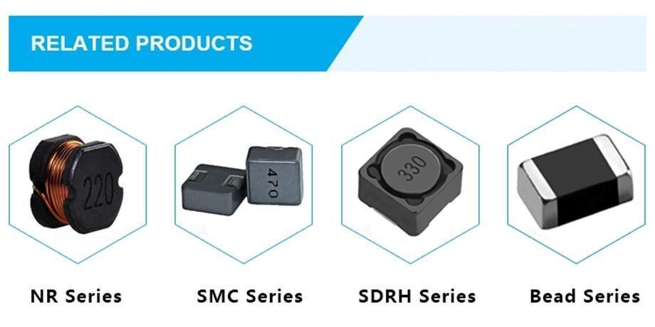
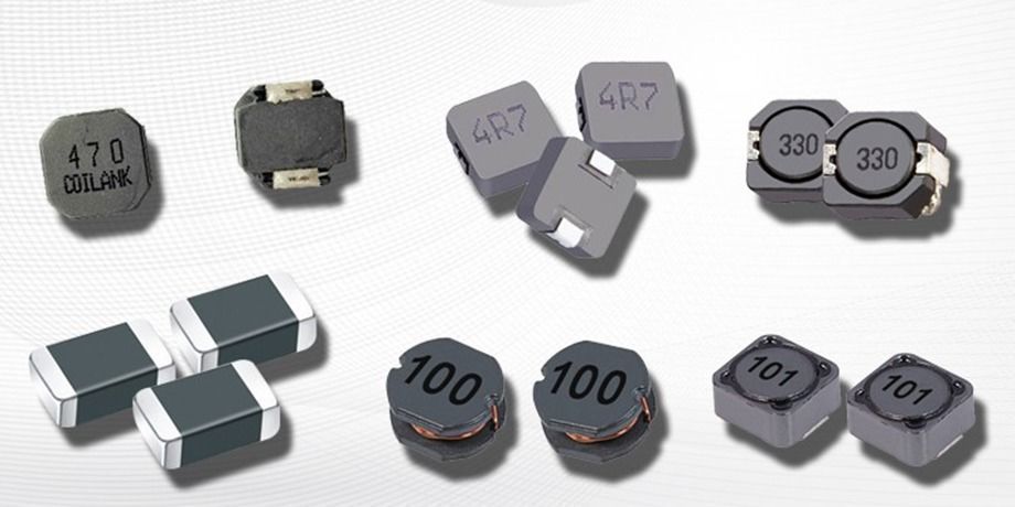
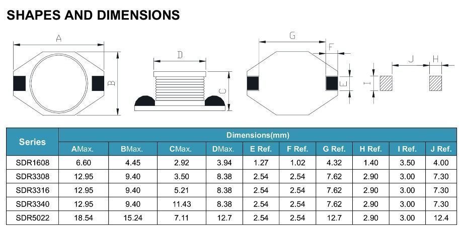
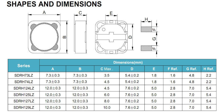
SMD/SMT Inductor(Coils)
An SMD inductor is a surface mount device inductor. It is a model of inductor that has no wire leads on its ends. This type of inductor is mounted directly to the surface of a circuit board via tining or soldering. They are positive reactance devices, available in many sizes and form factors optimized for particular applications. They are used in circuits that require filtering, power supplies, and many other functions. Inductance is associated with any PCB trace, via and ground plane and is usually considered a parasitic effect in all passive components and integrated circuits with wire bonds.ve components and integrated circuits with wire bonds.
Features:
â–ªIntegrally molded Power Inductor using a metallic magnetic material.Magnetic shield type and low noise
â–ªIt achieve large current,low Rdc,and compactness
â–ªGood performance in high-temperature environments with good DC superimposition characteristics
â–ªNo Halogen,RoHS compliant
Application:
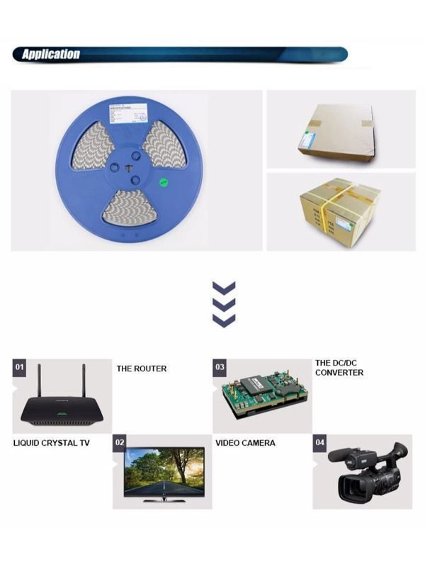
Power supply around the PC,servers,communication devices,automotive electronics,compact power supply modules,others.




FAQ
1-MOQ?
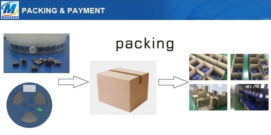
We will work hard to fit your MOQ .Small purchase quantity is ok.
2-Payment term?
T/T, Western Union, Paypal, Credit Card
3-Delivery port?
Shenzhen, Guangzhou, Zhongshan, Hongkong.
4-Shipping date?
About 7 days when we check the payment.
5-Do you produce the core and bobbin by yourself .
Yes.we have 2 head company,1 subsidiary company.one is bobbin factory,one is core factory,last one is transformer factory.
6-Where is your factory?
In ShaanxI
Smd Inductor,Smd Power Inductor,Smt Power Inductor,Copper Wire Smd Inductor
Shaanxi Magason-tech Electronics Co.,Ltd , https://www.magason-tech.com