Hello, everyone, and it's time for daily learning. Today we'll talk about two ways to use RAM in FPGA design. RAM is used to store random variables in the program's running data space. You can use Quartus II when you use it. The LPM function enables RAM customization.
Software Environment: Quartus II 11.0
Operating system: win7 
Implementation Method 1. Use LPM_RAM:
1. First prepare the memory initialization file, the .mif file.
How to generate a mif file? as follows:
The mif file is the memory initialization file, ie, the memory initialization file, used to configure the data in RAM or ROM. Generate the available mif files in Quartus II 11.0 in the following ways:
Method A: Using the Quartus Mif Editor
Advantages: For small-capacity RAM can quickly and easily complete the editing of mif files, without the need for third-party software editing;
Disadvantages: Once the amount of data is too large, one by one input can cause people to crash;
Usage: In quartus, [file]/[new], select Memory Initialization file, the following window pops up: 
Number of words: Number of addressable storage units. For 8bit address lines, select 256 here.
Words size: memory unit width, 8 bits
Then click on "OK". 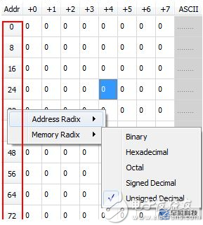
* Enter initialization data in the form;
* Right-click on the left address value, you can modify the address and data display format;
* The address of any data in the table = column value + row value, as shown in the blue cell address = 24 + 4 = 28;
After filling in the initial value for each unit, save the file.
Method B: Generated using mif software
No matter what editor you use, you must ensure that the format of the mif file is as follows: the left side of the colon is the address, the right side is the data; the semicolon ends;
DEPTH = 256;
WIDTH = 8;
ADDRESS_RADIX = HEX;
DATA_RADIX = HEX;
CONTENT
BEGIN
0000 : 0000;
0001 : 0000;
0002 : 0000;
... (there is a thousand words *.* omitted here)
00FA : 00FF;
00FB : 00FF;
00FC : 00FF;
00FD : 00FF;
00FE : 00FF;
00FF : 00FF;
END;
A mif generator is recommended here: Mif_Maker2010.exe, which can be downloaded from Baidu; software usage is as follows:
1. Open the software, [File]/[New];
2. Set the global parameters: 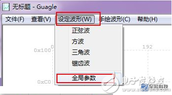
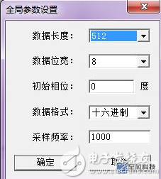
3. Generate waveforms:
Take a sine wave as an example: [Set Waveform]/[Sine Wave] 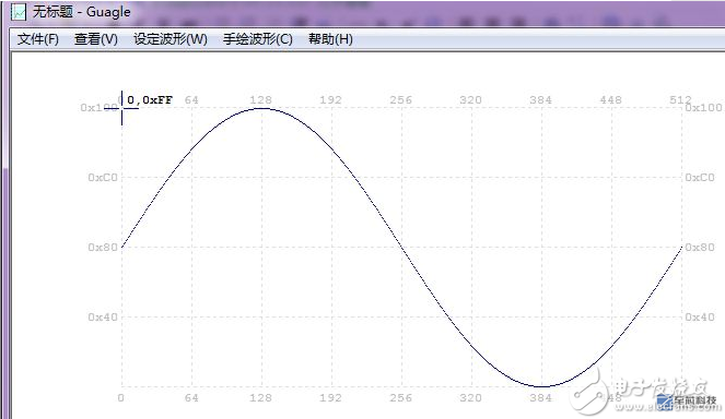
4. Modify the waveform:
[Hand-painted waveform]/[Line], left mouse button selects two starting points, the right mouse button ends, and you can draw an arbitrary waveform.
After the drawing is completed, select [Hand-painted Waveform]/[Cancel Hand-painted] again to end the drawing state. 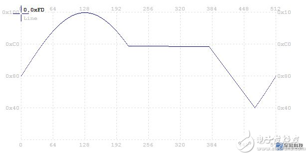
5. Save the file.
Method C: Using High-Level Languages
Generated using C language or matlab language, C language generated code is as follows: This code generates a sine wave data waveform, saved in TestMif.mif.
#include
#include
#define PI 3.141592
#define DEPTH 128 /*Data depth, the number of storage units */
#define WIDTH 8 /* width of storage unit */
Int main(void)
{
Int i,temp;
Float s;
FILE *fp;
Fp = fopen("TestMif.mif","w"); /*The filename is arbitrary, but the extension must be .mif*/
If(NULL==fp)
Printf("Can not creat file!");
Else
{
Printf("File created successfully!");
/*
* Generate file header: Be careful not to forget ";"
*/
Fprintf(fp,"DEPTH = %d;",DEPTH);
Fprintf(fp,"WIDTH = %d;",WIDTH);
Fprintf(fp,"ADDRESS_RADIX = HEX;");
Fprintf(fp,"DATA_RADIX = HEX;");
Fprintf(fp,"CONTENT");
Fprintf(fp,"BEGIN");
/*
* Output addresses and data in hexadecimal */
For(i=0;i {
/* Period of 128 points sine wave */
s = sin(PI*i/64);
/* Extends the value of the sine wave between -1 and 1 to 0-255*/
Temp = (int)((s+1)*255/2);
/* Output address and data in hexadecimal*/
Fprintf(fp,"%x:%x;",i,temp);
}//end for
Fprintf(fp,"END;");
Fclose(fp);
}
}
Verify that the generated data is correct: Open the generated mif file with Notepad and open the mif file with Quartus as follows: 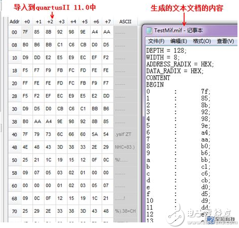
Can import successfully, and the data is consistent, indicating that the generation is correct.
After the use of the above recommended software and the creation of mif files, the next design was started.
This paper pre-generated a sine wave data file, TEST1.mif, which can be opened in Quartus II to view the content: [file]/[open], select memory files in the file type, and open TEST1.mif. The content is as follows: 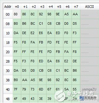
2. Generate LPM_RAM blocks
1) In the Quartus II, [tools] / [megawizard plugin manager], open the wizard, select the RAM under the [memory compiler] folder: select single-port RAM here,
Namely: RAM: 1-PORT, named RAM1P: 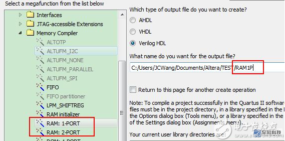
2) Set the memory depth to 128, the data width to 8 bits, select the embedded M4K RAM implementation, and use the single clock scheme: 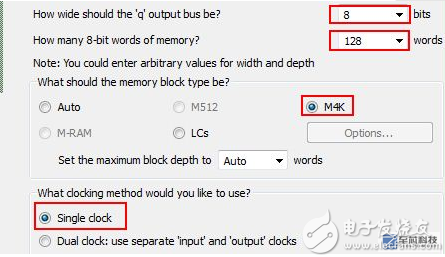
3) Deselect the "data output latch" and do not need the clock enable terminal: 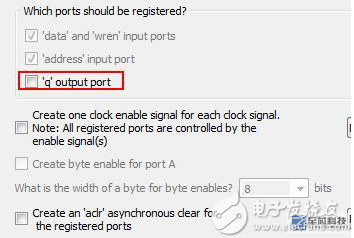
4) Use mif to initialize the RAM block, allow "Read and write in system memory", and set this RAM's ID to RAM1:
* Load the previously generated memory initialization file: TEST1.mif;
* ID is mainly used for multi-RAM system, the identification of different RAM, here named RAM1;
* Regarding the meaning of “reading and writing in system memoryâ€, an article will be added in the follow-up to introduce the use of the tool. 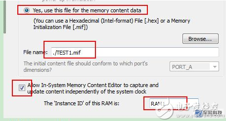
After the above settings, a file named RAM1P.v can be generated and can be instantiated and used later.
3. Instantiate RAM1P.v and use it. The instantiation method is as follows:
Module TEST (
Input [6:0] address,
Input clock,
Input [7:0] data,
Input wren,
Output [7:0] q
);
RAM1P RAM1P_inst (
.address ( address ),
.clock ( clock ),
.data ( data ),
.wren ( wren ),
.q (q )
);
Endmodule
It is recommended to use verilog texts for instantiation, and it is strongly disfavored to instantiate each module in a schematic manner.
Generated RTL diagram: 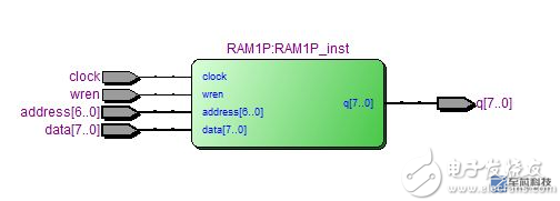
4. Simulate the RAM block to understand the characteristics of the port: 
* Since the clock scheme used is a single clock, Q outputs the data in the address specified by address regardless of wren=0 or 1. This can be seen from the verilog description. This is done using the assign statement (verilog code) as follows).
* When wren=1, the data at the data input is written to the memory location specified by address.
The output data is 0x80, 0x86, 0x8c, 0x92,... In contrast to the contents of the mif file shown above, you can verify that the mif file has been successfully imported;
The next output data 0x0c, 0x0d, 0x0c, 0x0c, is written in the address 04, 05, 06, 07 by the data input data during wren = 1;
Then continue to output 0xb0, 0xb6 ..., it is still the initial data of the corresponding address in the mif.
Note: In the compilation process, if you use the Cyclone II device, an error "Error: M4K memory block WYSIWYG primitive ..." may appear. The solution is:
[ASSIGNMENTS]/[SETTING], find the following location, enter "CYCLONEII_SAFE_WRITE" in name and "VERIFIED_SAFE" in DEFAULT SETTING;
Then click the add button: 

Method two, using verilog plain text description:
Generate the same function of the RAM block, the code is as follows:
Module RAM1P (
Input [6:0] address,
Input clock,
Input [7:0] data,
Input wren,
Output [7:0] q
);
(* ram_init_file = "TEST1.mif " *) reg [7:0] mem[127:0];
Always@(posedge clock)
If(wren) mem[address] <= data; /*Write data on the rising edge of the clock */
Assign q = mem[address];
Endmodule
Note that the method of loading the mif file into RAM at this time is implemented by means of text description. This method has the disadvantage that it cannot be simulated in modelsim:
(* ram_init_file = "TEST1.mif " *) reg [7:0] mem[127:0];
Compare the advantages and disadvantages of the two methods: 
After QuartusII's compilation report can be seen, the second method compared to the method one, taking up a lot of LE, while also using 1024 registers, so the second method is very uneconomical, given here is only to provide a reference, easy to understand The working mode of LPM_RAM is usually recommended to use method 1 to construct RAM when it is used normally.
Talk to you today, everyone, come on. ;i++)
72V Battery Pack ,Lithium Ion Battery Pack,Lithium Battery Pack,Battery Power Pack
Zhejiang Casnovo Materials Co., Ltd. , https://www.casnovonewenergy.com