In terms of people's understanding, polymer conductive films are used as electrical conduction media for multi-layer plate holes. It is not a mature product. People think that the physical properties are not good enough. In fact, it is understandable that such understanding is true. The operability and quality performance of high-lead products are still uneven.

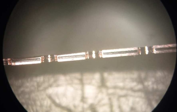
One of the typical problems: part of the hole copper caused by the difference in resistance of the multilayer board hole is too thin, making the thermal shock resistance very poor, and even the temperature of the reflow solder can not cause the thin copper hole to break,
At present, although there are many companies that have introduced polymer conductive film products, most products still have problems in achieving the hole conduction of multilayer boards. Specifically, the resistance value between the inner layer copper of the multilayer board and the substrate is too large and uneven, which reduces the efficiency of copper plating thickening. This is a fatal defect. Defective holes are often conductive during electrical measurement. Passable. However, due to the high temperature of the SMT assembly process, the hole copper is too thin to withstand thermal shock and breaks. Many board manufacturers have used the high-conductivity products indiscriminately. Secco has systematically improved this defect from product design to application control. Mainly through the improvement of product design to improve the potential difference between the inner layer copper of the multilayer board and the insulating substrate of the hole wall after adjusting the electric charge, and to improve the uniformity of the bath liquid in the conductive process and reduce the aging rate to achieve uniform coating, to ensure that the resistance value is low and consistent . Completely put an end to this problem. For example, Shenzhen Yisheng Circuit, Dongguan Pinsheng, Meizhou Jianghong and other multi-layer board factories have proved the reliable performance of SECOT products after long-term use and comparison.
Typical problem two: It is considered that the hole wall of the PCB and the hole copper have a poor bonding force.
In fact, the poor binding force is consistent with such problems in the traditional PTH process. After the drilling is completed, if the deburring cleaning is insufficient, the dust on the hole wall is not cleaned. This kind of problem is most likely to occur. Often, the polymer conductive film is only processed by the deburring process in the front stage cleaning process, and the water washing process is far away. It is not as long and thorough as the vertical line cleaning process, and the slot holes are more obvious due to the large roughness. To solve this problem, it is necessary to ensure sufficient water washing and increase the process of removing slag to bite the dust, glue slag and loose layer on the surface of the hole wall to ensure the bonding force of the hole copper. Then do the polymer conductive process to solve it.
Secco's hole-wall binding force for polymer conductive membranes was compared with that of traditional PTH in a third-party testing agency. The pull-out force PTH of the same type of holes is 95 pounds, and the polymer conductive membrane is 103 lbs. Facts prove that the combination with PTH is slightly better than the traditional process.
In addition, after two years of quality tracking, we found that the board processed by Sai Kete's high-conductivity products has almost no copper in the holes and no conduction in the holes, which is significantly better than the traditional PTH process.
After two years of product performance in the market. Sacco's polymer conductive film has been widely used in the hole conduction process of multilayer boards, which is a qualitative breakthrough in domestic high-conductivity products.
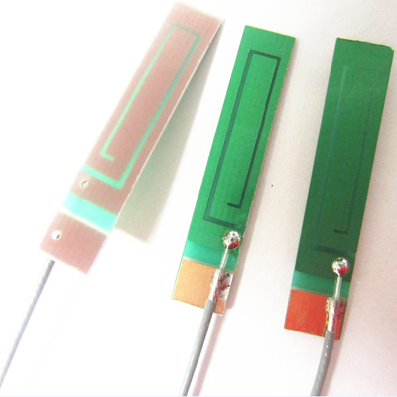
- The Description of PCB/FPC/Ceramic Antenna
Cellular /WiFi multi-band embedded flexible PCB antenna
It is equivalent to pulling out the antenna line on the PCB board and using other external metals to do the antenna. It is usually used in medium and low end mobile phones with complex frequency band and smart hardware products.
Advantages: suitable for almost all small electronic products, can do more than ten frequency band of complex antennas, good performance, low cost.
Disadvantages: need to be debugged separately for each product.
The Picture of PCB/FPC/Ceramic Antenna

pcb antenna,5g pcb antenna,lte pcb antenna,lte pcb antenna,2.4g pcb antenna
Yetnorson Antenna Co., Ltd. , https://www.yetnorson.com