The Spartan-6 clock routing network includes a global clock network driven by BUFGMUX and an I/O area clock network driven by an I/O clock buffer (BUFIO2) and a PLL clock buffer (BUFPLL).
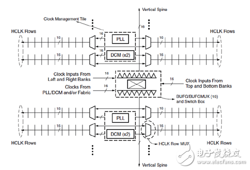
(1) Global clock network.The Spartan-6's global clock network is driven by 16 BUFGMUXs located in the center of the chip. There are three types of input signals for BUFGMUX.
Clock input for the top and bottom BANK.
Clock input for BANK on the left and right.
FPGA internal interconnect and / or PLL / DCM.
These three resources are switched by the switching module in the center of the chip.
Each BUFGMUX output drives a vertical clock ridge along which the horizontal clock HCLK is traversed.
There are two types of HCLK inputs, which are switched by a dedicated multiplexer.
The output of BUFGMUX.
The output of the PLL or DCM, each HCLK corresponds to one PLL or two DCMs.
Since there are 32 global clock input pins and 16 global input buffers in Spartan-6, it is possible that two clock input pins drive a global clock. When the global clock buffer (BUFG or BUFGMUX) is directly driven through the global clock pin (IBUFG or IFUFGDS), BANK0, BANK1 and BANK5 share 8 global clock buffers. Similarly, BANK2, BANK3 and BANK4 share 8 global clocks. Buffer, as shown in Figure 2-14.

Figure 2-14 Spartan-6 FPGA global clock structure
To increase wiring flexibility, BUFIO2 can be used as the second global clock buffer when using the second BUFIO2. Since system resources are optimized according to the primary BUFIO2 path, system performance is affected for global clocks that do not use the primary BUFIO2 resource.
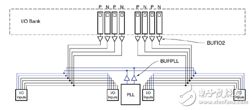
(2) I/O area clock network.As shown in Figure 2-15, an I/O clock network can be driven by the PLL through the BUFPLL. Each PLL has two associated buffers that extend to the entire I/O BANK.

I in FIGS. 2-15 Spartan-6 FPGA I / O BANK / O clock structure
Each BANK has two separate I/O clock regions, and each half of the I/O Bank has four high-speed I/O clocks driven by four dedicated BUFIO2 buffers.
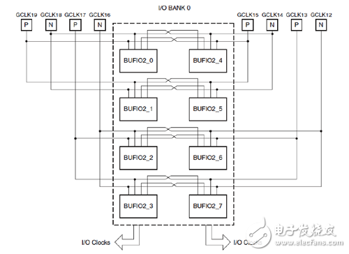
The I/O clock input pin can be extended to the entire BANK through BUFIO2, as shown in Figure 2-16. Use two BUFIO2 resources, such as BUFIO2_0 and BUFIO2_4, to extend the clock to the entire BANK.

Figure 2-16 I/O clock in I/O BANK
When the input delay is enabled, one input pin cannot drive two BUFIO2 buffers. In addition to providing input pins to the I/O clock network, BUFIO2 also provides dedicated clock paths to PLL/DCM and BUFG.
I-Beam Inductors,Chip Inductors,Color Ring Inductor,R-Bar Inductors
Shenzhen Sichuangge Magneto-electric Co. , Ltd , https://www.scginductor.com