This paper introduces a design scheme of 12V new intrinsically safe power supply based on TOP244Y. The core of the system uses Power IntegraTIon's switching power supply chip TOP244Y. On the basis of the switching power supply, an overvoltage protection circuit and an overcurrent protection circuit are applied to stabilize the voltage at 12V. After voltage protection test and overcurrent protection test verification, The power supply satisfies the intrinsic safety requirements, thus confirming the feasibility of this solution.
1 Introduction
In recent years, China's coal mine mechanization and automation have been increasing, and mine monitoring, communication, instrumentation automation systems and other applications are becoming more and more common, but the special environment of coal mines requires that coal mine electrical equipment must use intrinsically safe equipment. The intrinsically safe power supply is an indispensable part of the mine intrinsically safe system. Its technological advancement and product quality determine the reliability of the intrinsically safe equipment, which directly affects the accuracy and stability of the monitoring system data collection, and is related to mine safety. Production, resilience and miners' safety.
2. System overall plan
According to the standard of DC stabilized power supply for coal mine, the input voltage of the power supply is 75%~110% of the nominal value of AC 127V (ie 95V~140V), and the ripple voltage of the output voltage should not exceed 5% of the DC output voltage of 12V. Requirements, this article uses TOP244Y switching power supply chip, on the basis of high-frequency switching power supply, plus overvoltage protection circuit, overcurrent protection circuit, designed a new 12V intrinsically safe power supply (highest open circuit voltage 12.4V, maximum short circuit current 150mA) .
As shown in Figure 1, the system includes the following three parts:
Switching power supply circuit, overvoltage protection circuit, overcurrent protection circuit.

3. Hardware circuit design
3.1 switching power supply circuit
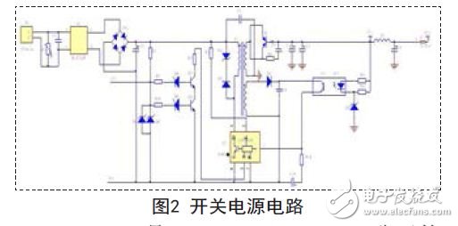
The switching power supply circuit converts the alternating current 127V into a direct current 23V. The circuit schematic is shown in Figure 2. The alternating current is rectified and filtered to become a DC with large ripple. The high frequency transformer and the switching power supply chip TOP244Y get 23V DC.

TOP244Y is Power IntegraTIon's TopSwitch II series, which is easy to implement optimized design of switching power supply. The designed AC input voltage range is 85V~265V. It can realize input undervoltage protection, overvoltage protection and external limiting current. Reduce the maximum duty cycle and other functions. TOP244Y has frequency jitter characteristics, which is very helpful in reducing electromagnetic interference.
The 1 pin of TOP244Y is used for duty cycle control. The duty cycle is changed according to the feedback voltage to adjust the voltage stable output. The 2 pin provides automatic monitoring and adjustment of line voltage overvoltage and undervoltage. The 3 pins are usually connected to the triode. Realize remote switch control, when the triode is turned on, 3 pins are grounded, TOP244Y works normally, when the triode is disconnected, 3 pins are suspended, TOP244Y is disabled; 4 pins are the source of TOP244Y internal MOSFET, 6 pins It is the drain of the internal MOSFET, used as a switch, and is supplied to the high-frequency transformer; 5 pin is the frequency pin, and the working switching frequency of TOP244Y is 132KHz when grounding. R3 is an undervoltage or overvoltage detection resistor and can provide the line. Voltage feedforward to reduce fluctuations in switching frequency. D2 and D3 form a drain clamp circuit, which can absorb the spike voltage generated by the primary leakage inductance of the high-frequency transformer T1 when the internal MOSFET is turned off, and protect the MOSFET from damage. Resistor R5 is used to externally set the drain limit current of the power switch tube to be slightly higher than the drain peak current at full load or input undervoltage, which allows the output load to be unstable or not appearing during power supply startup. In the case of saturation, a small-sized high-frequency transformer is used. When the input DC voltage is overvoltage, R5 can also automatically reduce the maximum duty cycle Dmax, limiting the maximum load power.
The precision optocoupler feedback circuit consists of a linear optocoupler PC817A, a Zener diode D7, and resistors R6 and R8. The output voltage Uo is changed by the optocoupler to change the 1-pin current IC of the TOP244Y, so that the duty ratio changes, and the Uo remains unchanged. The output voltage of the feedback winding is rectified and filtered by D3 and C8 to provide a bias voltage to the receiving tube in the optocoupler. C10 also forms a spike voltage filter with R14 to keep the bias voltage constant when the load is heavy.
3.2 Overvoltage protection circuit

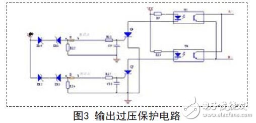
As shown in Figure 3, when the output voltage 12V increases for some reason (assuming it is increased to 13V), the D11 and D13 regulators are turned on, triggering the fast thyristors Q4 and Q6, respectively, and turning on the photocouplers U2 and U4. The base level of the transistors Q2 and Q3 connected through points A and B is pulled to a low level to realize remote disabling control of the switching power supply chip TOP244Y, TOP244Y stops working, the VCC voltage is zero, and the final output voltage is zero. Achieve output overvoltage protection. The role of R11 and R15 in the figure is to reduce the bias current at the input of the fast thyristor.
Flat Wire Common Mode Inductors
Flat Wire Common Mode Inductors,Vertical Low Profile Common Mode Inductors,Horizontal Flat Wire High Current Inductor,Flat Copper Wire Common Mode Inductors
Shenzhen Sichuangge Magneto-electric Co. , Ltd , https://www.rodinductor.com