Abstract: This application note discusses how to select appropriate transformers and passive components, and to obtain a wider input frequency response gain flatness without sacrificing the dynamic performance of high-speed ADCs.
For higher IF analog-to-digital converters (ADCs), correct selection of board-level components is a necessary condition for high dynamic performance and wide gain flatness. This technical document describes how to select the input network and simplify the design of single-ended to differential signal conversion with the help of broadband transformers, termination resistors and filter capacitors.
This article takes MAX1449 as an example for explanation and analysis, and gives two possible input configurations. Figure 1 shows a typical AC-coupled, single-ended to differential conversion design. This design uses a broadband transformer (such as Mini-Circuits' T1-1T-KK81 (200MHz)), and the primary side is terminated with a 50Ω resistor and a 25Ω / 22pF filter network. In this configuration, a single-ended input signal with a source impedance of 50Ω is converted into a differential signal by a transformer. 50Ω primary-side termination can achieve a good match between the signal source and the transformer. However, this also means that there is a mismatch between the primary and secondary sides of the transformer. The equivalent resistance of the primary side is 25Ω, but there is a large impedance mismatch on the secondary side. This is because the ADC's 20kΩ input resistance is paralleled with a 22pF capacitor. This will affect the frequency response characteristics of the input network, and ultimately the frequency response characteristics of the converter. The nominal leakage inductance of the transformer is 25nH to 100nH. Combined with a 22pF input filter capacitor, this will produce a resonant frequency:

Resonant frequencies between 110MHz and 215MHz will produce interference spikes in this band.
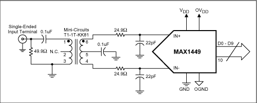
figure 1.
Figure 2 depicts a similar AC-coupled configuration, but it uses a broadband transformer with primary-side termination and better performance (such as Mini-Circuits' ADT1-1WT (800MHz)) and a 25Ω / 10pF filter network. Although the impedance of the ADT1-1WT is 75Ω, the lower leakage inductance raises the -1dB frequency to 400MHz, while the T-1T-KK81's -1dB frequency is only 50MHz.
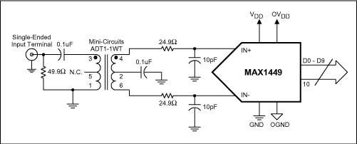
figure 2.
Figure 3 shows the comparison results of the two termination architectures supplemented by transformers and filter network devices. From the figure we can see a significant performance improvement. The input bandwidth of the T1-1T-KK81 transformer (blue line) has a gain fluctuation of approximately 0.5dB between 90MHz and 110MHz, while the input bandwidth of the ADT1-1WT transformer (purple line) maintains a gain fluctuation of 0.1dB within 300MHz. Dynamic range (ADT1-1WT transformer, 50Ω
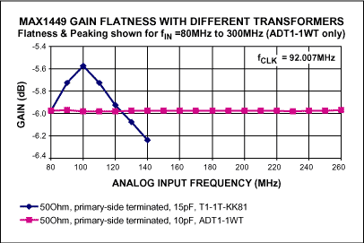
image 3.
The primary side is terminated, and the input filter capacitor at INP and INN is 10pF). At fIN = 50MHz, the SNR is still 58.4dB. Although Figure 3 only shows the input frequency of 80MHz to 260MHz (ADT1-1WT), laboratory test results show that the input frequency can exceed the 8th order Nyquist frequency within a range of 0.1dB of gain fluctuation.
Improving transformer secondary impedance matching can further improve gain flatness. One method is to use secondary termination instead of primary termination. This method will be discussed in other application notes. This solution is based on Maxim's recently introduced MAX1122 / 23/24 series for input network design and analysis. Please refer to the following application note link for details on primary and secondary termination.
Reference MAX1448EVKit Datasheet, Rev1, 7/2001, Maxim Integrated Products, Sunnyvale, CA
MAX1449 Datasheet, Rev0, 10/2000, Maxim Integrated Product, Sunnyvale, CA
Application note: Secondary-side transformer termination improves gain flatness of high-speed ADCs
For higher IF analog-to-digital converters (ADCs), correct selection of board-level components is a necessary condition for high dynamic performance and wide gain flatness. This technical document describes how to select the input network and simplify the design of single-ended to differential signal conversion with the help of broadband transformers, termination resistors and filter capacitors.
This article takes MAX1449 as an example for explanation and analysis, and gives two possible input configurations. Figure 1 shows a typical AC-coupled, single-ended to differential conversion design. This design uses a broadband transformer (such as Mini-Circuits' T1-1T-KK81 (200MHz)), and the primary side is terminated with a 50Ω resistor and a 25Ω / 22pF filter network. In this configuration, a single-ended input signal with a source impedance of 50Ω is converted into a differential signal by a transformer. 50Ω primary-side termination can achieve a good match between the signal source and the transformer. However, this also means that there is a mismatch between the primary and secondary sides of the transformer. The equivalent resistance of the primary side is 25Ω, but there is a large impedance mismatch on the secondary side. This is because the ADC's 20kΩ input resistance is paralleled with a 22pF capacitor. This will affect the frequency response characteristics of the input network, and ultimately the frequency response characteristics of the converter. The nominal leakage inductance of the transformer is 25nH to 100nH. Combined with a 22pF input filter capacitor, this will produce a resonant frequency:

Resonant frequencies between 110MHz and 215MHz will produce interference spikes in this band.

figure 1.
Figure 2 depicts a similar AC-coupled configuration, but it uses a broadband transformer with primary-side termination and better performance (such as Mini-Circuits' ADT1-1WT (800MHz)) and a 25Ω / 10pF filter network. Although the impedance of the ADT1-1WT is 75Ω, the lower leakage inductance raises the -1dB frequency to 400MHz, while the T-1T-KK81's -1dB frequency is only 50MHz.

figure 2.
Figure 3 shows the comparison results of the two termination architectures supplemented by transformers and filter network devices. From the figure we can see a significant performance improvement. The input bandwidth of the T1-1T-KK81 transformer (blue line) has a gain fluctuation of approximately 0.5dB between 90MHz and 110MHz, while the input bandwidth of the ADT1-1WT transformer (purple line) maintains a gain fluctuation of 0.1dB within 300MHz. Dynamic range (ADT1-1WT transformer, 50Ω

image 3.
The primary side is terminated, and the input filter capacitor at INP and INN is 10pF). At fIN = 50MHz, the SNR is still 58.4dB. Although Figure 3 only shows the input frequency of 80MHz to 260MHz (ADT1-1WT), laboratory test results show that the input frequency can exceed the 8th order Nyquist frequency within a range of 0.1dB of gain fluctuation.
Improving transformer secondary impedance matching can further improve gain flatness. One method is to use secondary termination instead of primary termination. This method will be discussed in other application notes. This solution is based on Maxim's recently introduced MAX1122 / 23/24 series for input network design and analysis. Please refer to the following application note link for details on primary and secondary termination.
Reference MAX1448EVKit Datasheet, Rev1, 7/2001, Maxim Integrated Products, Sunnyvale, CA
MAX1449 Datasheet, Rev0, 10/2000, Maxim Integrated Product, Sunnyvale, CA
Application note: Secondary-side transformer termination improves gain flatness of high-speed ADCs
Dc Motor Controller,Brushless Motor Controller,Ti Bldc Motor Controller,Brushless Dc Motor Controller
Jinan Keya Electron Science And Technology Co., Ltd. , https://www.keyaservo.com