Please SSD basic working principle
Starting from the host PC, the user requests the SSD from the operating system application level. The file system converts the read and write requests to corresponding read/write and other commands that comply with the protocol. The SSD receives commands to perform the corresponding operations and then outputs the results. The input and output of each command are standardized by the protocol standards organization. This is the standard thing. It is the same as HDD except that HDD is replaced with SSD hardware to store data and the accessed object becomes SSD.

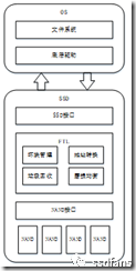
Figure 1-13 SSD system call
The input of the SSD is a command and the output is Data and Command Status. The Front End of the SSD receives user command requests and passes the internal calculation and processing logic to output the data or status required by the user.
As you can see from Figure 1-13, SSDs consist of three major functional modules:
1. Front-end interface and related protocol modules;
2. The middle Flash Translation Layer (FTL) module;
3. Backend and flash memory communication modules.
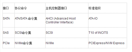
The SSD front end is responsible for direct communication with the host and receives commands and related data sent by the host. After the command is processed by the SSD, it is finally passed to the front end to return command status or data to the host. SSDs are connected to hosts through interfaces such as SATA, SAS, and PCIe to implement the corresponding AHCI, SCSI, and NVMe protocols.
Table 1-1 SATA/SAS/PCIe Interface Protocols

Let's take a look at how SSDs read and write.
The host sends a write command to the SSD through the interface. The SSD executes the command and receives the data to be written by the host. Data is generally cached in the internal SSD of the SSD. The FTL allocates a flash address for each logical block. After the data is concatenated to a certain amount, the FTL will send a write flash request to the back end, and the back end will then respond to the write request. , write the data in the cache to the corresponding flash memory space.
Because Flash cannot overwrite writes, Flash blocks must be erased to write. A block of data sent by the host, it is not written in a fixed location on the flash, SSD can be assigned to any possible flash space to write. Therefore, the SSD needs such an internal FTL to complete the conversion or mapping of logical data blocks to flash physical space.
For example, assume that the SSD has a capacity of 128 GB and the logical block size is 4 KB, so the SSD has a total of 128 GB/4 KB = 32 M logical blocks. Each logical block has a mapping, ie each logical block has a storage location in flash memory space. If the flash address size is represented by 4 bytes, 32M*4B=128MB size mapping table is required to store 32M logical data blocks in the flash memory.
It is because the SSD internally maintains a mapping table from logical address to physical address translation. When the host sends a read command, the SSD can search the mapping table according to the logical data blocks that need to be read to obtain the logical data in the flash memory space. At the location, the back end can read the corresponding data from the flash memory into the SSD internal cache space, and the front end is responsible for returning this data to the host.
Since the front-end interface protocols are standardized, the interfaces and operations of the back-end and flash memory are standardized (flash memory follows the ONFI or Toggle protocol). Therefore, after an SSD is defined in the front-end protocol and flash memory, the difference is reflected in the FTL algorithm. Now. The FTL algorithm determines the core parameters of the SSD such as performance, reliability, and power consumption.
In fact, FTL needs to do a lot of other things in addition to the mapping of logical data to flash space.
As mentioned earlier, flash memory cannot overwrite writes, so as user data continues to be written, flash space can generate junk (invalid data). FTL needs to do Garbage Collection to free up available flash space for writing user data.

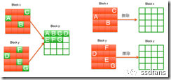
Figure 1-14 Recycling of garbage data
Take Figure 1-14 as an example. There are a lot of garbage data on Block x and Block y. Among them, A, B, and C are valid data on Block x, and D, E, F, and G are valid data on Block y. Garbage collection is to move one or more valid data from a block and write it to a free block (such as Block z). When the valid data on these blocks are all removed, the FTL can erase these blocks, and then the blocks can be used again for the SSD to write new data.
In addition, flash memory is a life span. Each flash block cannot write data all the time. Therefore, in order to ensure the maximum amount of data to be written, FTL must write each flash block as evenly as possible. This is called wear leveling. .
In addition, FTL also needs to implement such things as bad block management, read disturb processing, data hold processing, error handling, and so on. Understand the FTL, SSD's working principle will be mastered. About FTL, this book has a special chapter introduction, the reader can skip to Chapter 4 to read.
1.2 SSD Product Core Parameters
Before purchasing SSDs, users will pay attention to some of its parameters, such as how fast they can run, what flash memory they use, and so on. In particular, enterprise-level users need to study SSD core indicators in an all-round way, resolve what indicators they are concerned about, how they are concerned, and compare competing products. Finally, one by one, the internal nature of products must be removed. This section takes the SSD product as an example and takes everyone together to interpret the core parameters of the SSD product.
Distribution System,Plastic Box With Splitter,Wall Mounted Fiber Terminal Box
ShenZhen JunJin Technology Co.,Ltd , https://www.jjtcl.com