The data acquisition system can collect various data and parameters in the production process in real time, and becomes a very important means to obtain the working status and operation of the system. In recent years, various application fields have put forward more stringent requirements on the performance of data acquisition systems: not only the function of collecting key information is required, but also the anti-interference ability of the acquisition system and the rejection ability of unwanted signals are put forward. Especially when the collected signal is covered by the unwanted signal or the acquisition system works in an environment with strong interference, how to extract the useful signal from the collected data and remove the interference signal is the difficulty and research hotspot of the current data acquisition system. FPGA-based FIR filter has become a very important means of digital signal extraction because of its flexible design, fast speed, easy gain control and good stability. Using it as the front-end signal processing of the data acquisition system has become a very good implementation in the field of high precision and anti-interference data acquisition.
Introduction to 1 FIR filterThe finite impulse response FIR (Finite Impulse Response) filter has been widely used in the field of digital signal processing due to its good linear phase and high stability. The basic system function of the N-order FIR filter is as shown in equation (1):
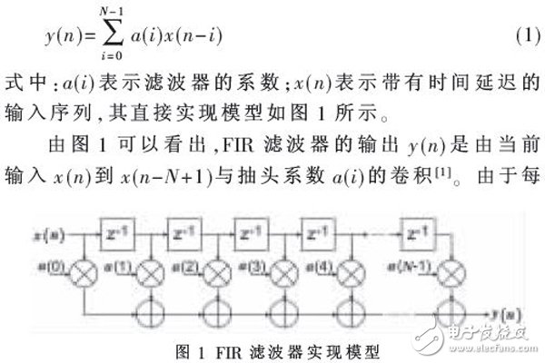
The output has to be N times multiplied and N-1 times added, so if it is implemented by a serial structure, when the order number N is large, the delay of the system will be large. Today's digital FIR filters can be roughly divided into DSP-based FIR filters and FPGA-based FIR filters: DSP-based FIR filters are simple to implement and can be implemented with only a few simple statements, and are used in large numbers for digital signals. During processing. However, since the DSP operation is serial, it is impossible to design a high-order fast FIR filter. FPGA-based FIR filter is a new type of FIR filter implementation developed in recent years with the rapid growth of FPGA resources [2]. It has strong configurability, flexibility, speed and stability. Advantages have gradually become the preferred implementation of FIR filtering in industrial control and aerospace.
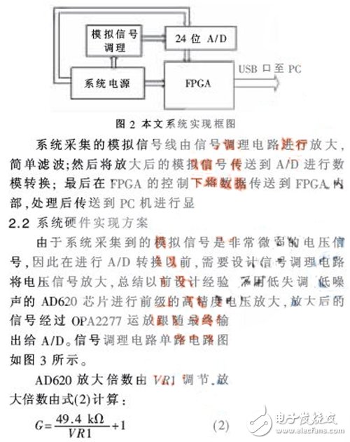
2 system implementation scheme 2.1 overall design schemeThe analog signal collected by the system is an undemodulated weak voltage signal with a large noise and sinusoidal signal. The system implementation block diagram is shown in Figure 2.
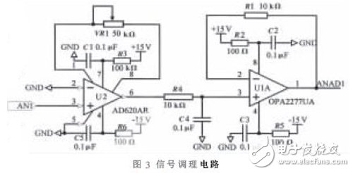
Adjust the sliding rheostat to control the output voltage of the OPA2277 within 0~5 V. Although a simple active RC low-pass filter is added, the signal useful component is still covered by noise and superimposed high-frequency sine wave.
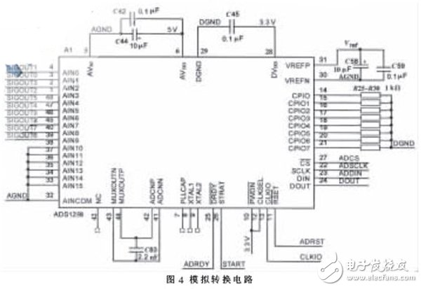
Although the amplified voltage signal is within 0~5 V, the key signal submerged in it is still only a few millivolts. If an ordinary low-precision ADC is used for analog-to-digital conversion, the conversion error of the ADC is just right and key. The signals are not much different, which introduces a relatively large error in the converted digital signal. Even after the subsequent filtering, the key signals superimposed with the error are obtained, and high-precision acquisition and demodulation cannot be realized. Therefore, the company's 24-bit 16-channel serial high-precision ADC chip ADS1258 is used for analog-to-digital conversion. The circuit diagram is shown in Figure 4.
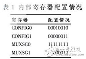
The main clock of the ADC adopts the 16 MHz square wave signal after the main clock of the FPGA is divided, and the AIN0~AIN9 channel is selected as the analog signal input, and the internal automatic scanning mode is adopted. The control ports of the ADC are connected to the general purpose I/O port of the FPGA. The ADC internal register configuration data is written from the FPGA through the SPI port of the ADC. Configuration data is written on the rising edge of the SPI clock, and the converted data is read on the falling edge of the SPI clock. The internal register configuration is shown in Table 1.
The main controller of this system adopts XILINX's SPARTAN3E series FPGA XC3S200E. This chip can meet the requirements of the system in terms of resources, and the most important thing is that in the development environment ISE 9.1 and later versions, the SPARTAN3E series chip system is It comes with a powerful FIR filter IP core, which makes it easy to design a high-speed, reliable, and low-resource FIR filter. The data is transferred to the host computer using CY7C68013. Since this design is not the focus of this system, it will not be described.
2.3 System ProgrammingProgramming is the key to this system. The key to the difference between the previous system is the use of high-precision ADC and the introduction of innovative FIR filtering, which makes the acquisition system capable of ultra-high precision and strong anti-interference.
The ADS1258 is a multi-channel serial ADC that is flexible because it is controlled by writing certain configuration data to its internal registers for A/D conversion. The configurable baud rate and chopping function also make the device more outstanding. The device control flow is shown in Figure 5.
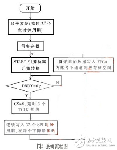
The read and write timing of the ADC is particularly important, so the delay of the transition between states must be controlled according to the chip data, which does not affect the conversion cycle and ensures the correct result. The delay of 218 TCLK cycles after the device is powered on must be guaranteed. Otherwise, although the chip can work, A/D conversion can be performed, but the write register naming cannot be used, and the configuration data required by the system cannot be written to each register. In the early stage of system development, because this long reset time was neglected, the write command could not be executed correctly. After adding the reset delay, the ADC works normally and the register data can be written smoothly. Each time a conversion is completed, 32-bit valid data [3] can be read from the chip SPI port. The data format is shown in Table 2.

Hf Drivers - Neodymium,Bullet Tweeter Speaker,Loud And Ultra Crisp Sound,Compression Driver
NINGBO BOILINGSOUND ELECTRONICS CO.,LTD , https://www.tweeterspeaker.com