With the development of modern processor technology, in the field of interconnection, the use of high-speed differential bus instead of parallel bus is the trend. High-speed differential signals can use higher clock frequencies than single-ended parallel signals, allowing fewer signal lines to be used to achieve the bus bandwidth previously required for many single-ended parallel data signals.
PCI Express is a new generation of bus interface. As early as the spring of 2001, Intel proposed to use a new generation of technology to replace the PCI bus and the internal connection of a variety of chips, and called the third generation I / O bus technology. Then at the end of 2001, more than 20 industry-leading companies including Intel, AMD, DELL, and IBM began drafting specifications for new technologies, which were completed in 2002 and officially named PCI Express. It uses the popular point-to-point serial connection in the industry. Compared to the shared parallel architecture of PCI and earlier computer bus, each device has its own dedicated connection, no need to request bandwidth to the entire bus, and can transfer data rate. Raise to a very high frequency to achieve the high bandwidth that PCI can't provide.
The PCI bus uses a parallel bus structure. All external devices on the same bus share the bus bandwidth. The PCIe bus uses a high-speed differential bus and uses an end-to-end connection. Therefore, only two connections can be made in each PCIe link. equipment. This makes the topology used by PCIe and PCI bus different. In addition to the PCI bus in the connection mode, the PCIe bus also uses some technologies used in network communication, such as supporting multiple data routing methods, multi-channel data transmission methods, and message-based data transmission methods. And fully consider the issue of quality of service (QoS) in the data transmission.

Unlike the PCI bus, the PCIe bus uses an end-to-end connection. Only one device can be connected to each other at both ends of a PCIe link. The two devices are data transmitting end and data receiving end. In addition to the bus link, the PCIe bus has multiple levels. The transmitting end will pass these layers when transmitting data, and the receiving end will also use these levels when receiving data. The hierarchy used by the PCIe bus is similar to the network protocol stack.
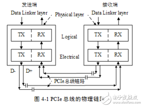
1.1 End-to-end data transferThe PCIe link uses "end-to-end data transmission mode", and both the transmitting end and the receiving end contain TX (transmission logic) and RX (reception logic), and its structure is as shown in FIG.

As shown in the above figure, in a data path (Lane) of the physical link of the PCIe bus, there are two sets of differential signals, which are composed of four signal lines. The TX component of the transmitting end and the RX component of the receiving end are connected by using a set of differential signals, which is also referred to as a transmitting link of the transmitting end, and is also a receiving link of the receiving end; and the RX component of the transmitting end and the TX component of the receiving end use another A group differential signal connection, also referred to as the receiving link of the transmitting end, and also the transmitting link of the receiving end. A PCIe link can consist of multiple Lanes.
The high-speed differential signaling electrical specification requires that its transmitter be connected in series with a capacitor for AC coupling. This capacitor is also known as an AC coupling capacitor. The PCIe link uses a differential signal for data transmission. A differential signal consists of two signals, D+ and D-. The signal receiving end compares the difference between the two signals to determine whether the transmitting end sends a logic "1" or a logic "0. ".
Compared with single-ended signals, differential signals are more resistant to interference because differential signals require "equal length", "equal width", "close", and are in the same layer. Therefore, the external interference noise will be “same†and “simultaneously†loaded onto the D+ and D- signals, and the difference is ideally 0, which has less effect on the logic value of the signal. Therefore differential signals can use higher bus frequencies.
In addition, the use of differential signals can effectively suppress electromagnetic interference EMI (Electro Magne TIc Interference). Since the differential signals D+ are close to D- and the signals are of equal amplitude and opposite polarity. The amplitudes of the coupled electromagnetic fields between the two lines and the ground line are equal and will cancel each other out, so the differential signal has less electromagnetic interference to the outside world. Of course, the disadvantages of the differential signal are also obvious. One is that the differential signal uses two signals to transmit one bit of data; the other is that the differential signal is relatively strict.
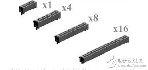
The PCIe link can be composed of multiple Lanes. Currently, the PCIe link can support 1, 2, 4, 8, 12, 16 and 32 Lanes, namely &TImes; 1, &TImes; 2, &TImes; 4, ×8, ×12 , x16 and x32 wide PCIe links. The bus frequency used on each Lane is related to the version used by the PCIe bus.
The first PCIe bus specification is V1.0, followed by V1.0a, V1.1, V2.0 and V2.1. The current specification for the PCIe bus is V2.1, and V3.0 is under development and is expected to be released in 2010. The bus frequency and link encoding methods defined by different PCIe bus specifications are not the same, as shown in Table 41.
Table 41 Relationship between PCIe bus specification and bus frequency and coding

As shown in the above table, the bus frequencies used by different PCIe bus specifications are not the same, and the data encoding methods used are different. The PCIe bus V1.x and V2.0 specifications use 8/10b encoding in the physical layer, ie 8 bits of valid data in 10 bits on the PCIe link; and the V3.0 specification uses 128/130b encoding, ie The 130 bit on the PCIe link contains 128 bits of valid data.
As shown in the above table, the V3.0 specification uses a bus frequency of only 4 GHz, but its effective bandwidth is twice that of V2.x. The V2.x specification is used as an example to illustrate the peak bandwidth that can be provided by PCIe links of different widths, as shown in Table 42.
Table 42 Peak Bandwidth of PCIe Bus

As shown in the above table, the x32 PCIe link can provide a link bandwidth of 160 GT/s, which is much higher than the peak bandwidth that the PCI/PCI-X bus can provide. The upcoming PCIe V3.0 specification uses a 4GHz bus frequency that will further increase the peak bandwidth of the PCIe link.
In the PCIe bus, the peak bandwidth of the PCIe link is calculated using GT (Gigatransfer). GT is the peak bandwidth delivered on the PCIe link, and its calculation formula is bus frequency × data bit width × 2.
In the PCIe bus, there are many factors that affect the effective bandwidth, so its effective bandwidth is difficult to calculate. Despite this, the effective bandwidth provided by the PCIe bus is much higher than the PCI bus. The PCIe bus also has its weaknesses, the most prominent of which is the transmission delay.
The PCIe link uses serial mode for data transfer. However, inside the chip, the data bus is still parallel. Therefore, the PCIe link interface needs to perform serial-to-parallel conversion. This serial-to-parallel conversion will generate a large delay. In addition, the data packets of the PCIe bus need to pass through the transaction layer, the data link layer and the physical layer. These data packets will also bring delays when crossing these layers.
Among PCIe bus-based devices, x1 PCIe links are the most common, while x12 PCIe links are rare, and x4 and x8 PCIe devices are rare. Intel typically integrates multiple x1 PCIe links into the ICH to connect to low-speed peripherals, while a M16 integrated PCIe link is integrated into the MCH to connect to the graphics controller. PowerPC processors are typically capable of supporting PCIe links of x8, x4, x2, and x1.
The data transmission between the physical links of the PCIe bus uses a clock-based synchronous transmission mechanism, but there is no clock line on the physical link. The receiving end of the PCIe bus contains a clock recovery module CDR (Clock Data Recovery), and the CDR will receive the message. The receiving clock is extracted to perform synchronous data transfer.
It is worth noting that in a PCIe device, in addition to the need to extract the clock from the message, the REFCLK+ and REFCLK- signal pairs are used as the local reference clock.
R&M BAR 9000 Puffs Disposable Vape Price is latest 9000 puffs with diamond shape, you can enjoy cool touch and lasting hit.Visual oil tank design with prefilled e liquid, carry pioneering direct vape technology, no pull plug, no filling, easy to use.Mesh coil inside, create smoother and bigger vapor.Flash RGB light blinking make you stand out when you suck.Bottom Type-c charging port and adjustable airflow control, perfect functionality.
Specifications:
- Capacity: 15ml
- 2%/5% nic salt by weight
- 9000 puffs per device
- Rechargeable battery
- RGB flash light
- OEM Available
RGB Light Disposable Vape,RM VAPE,Wholesale R&M Bar.
Shenzhen Essenvape Technology Co., Ltd. , https://www.essenvape.com